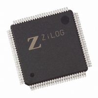
Z16C3010AEC Zilog, Z16C3010AEC Datasheet - Page 52

Z16C3010AEC
Manufacturer Part Number
Z16C3010AEC
Description
IC 10MHZ CMOS USC 100-VQFP
Manufacturer
Zilog
Series
USC®r
Datasheet
1.Z16C3010ASC00TR.pdf
(102 pages)
Specifications of Z16C3010AEC
Controller Type
USC Controller
Interface
DMA
Voltage - Supply
4.5 V ~ 5.5 V
Current - Supply
7mA
Operating Temperature
-40°C ~ 85°C
Mounting Type
Surface Mount
Package / Case
100-LQFP
Lead Free Status / RoHS Status
Contains lead / RoHS non-compliant
Available stocks
Company
Part Number
Manufacturer
Quantity
Price
Company:
Part Number:
Z16C3010AEC
Manufacturer:
HOLT
Quantity:
101
DS007902-0708
Notes:
accessible immediately after a hardware reset of the device. The first write to the USC,
after a hardware reset, programs the BCR. From that time on, the normal channel registers
may be accessed. No specific address need be presented to the USC for the BCR write
because the first write after a hardware reset is automatically programmed for the BCR.
In the multiplexed bus case, all registers are directly addressable through the address
latched by AS at the beginning of a bus transaction. The address is decoded from either
AD6–AD0 or AD7–AD1. This is controlled by the Shift Right/Shift Left bit in the BCR.
The address maps for these two cases are listed in
directly access the receive and transmit data registers (RDR and TDR) in the multiplexed
bus; if D/C is High the address latched by AS is ignored and an access of RDR or TDR is
performed.
In the nonmultiplexed bus case, the registers in each channel are accessed indirectly using
the address pointer in the Channel Command/Address Register (CCAR) in each channel.
The address of the desired register is first written to the CCAR and then the selected regis-
ter is accessed; the pointer in the CCAR is automatically cleared after this access. The
RDR and TDR are accessed directly using the D/C pin, without disturbing the contents of
the pointer in the CCAR.
Table 8. Multiplexed Bus Address Assignments
1. The Channel Reset bit in the CCAR places the channel in the reset state. To exit this
2. After reset, the transmit and receive clocks are not connected. The first thing that
The register addressing is listed in
registers are displayed in
Address Signal
Byte/Word Access
Address 4
Address 3
Address 2
Address 1
Address 0
Upper/Lower Byte Select
reset state either a word of all zeros must be written to the CCAR (16-bit bus), or a byte
of all zeros must be written to the lower byte of the CCAR (8-bit bus).
should be done in any initialization sequence is a write to the Clock Mode Control
Register (CMCR) to select a clock source for the receiver and transmitter.
Figure
P R E L I M I N A R Y
Shift Left
AD7
AD6
AD5
AD4
AD3
AD2
AD1
29.
Table 9
on page 50 while the bit assignments for the
Shift Right
AD6
AD5
AD4
AD3
AD2
AD1
AD0
Table
8. The D/C pin is still used to
Product Specification
Functional Description
Z16C30
48


