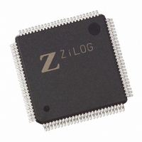
Z16C3010AEC Zilog, Z16C3010AEC Datasheet - Page 11

Z16C3010AEC
Manufacturer Part Number
Z16C3010AEC
Description
IC 10MHZ CMOS USC 100-VQFP
Manufacturer
Zilog
Series
USC®r
Datasheet
1.Z16C3010ASC00TR.pdf
(102 pages)
Specifications of Z16C3010AEC
Controller Type
USC Controller
Interface
DMA
Voltage - Supply
4.5 V ~ 5.5 V
Current - Supply
7mA
Operating Temperature
-40°C ~ 85°C
Mounting Type
Surface Mount
Package / Case
100-LQFP
Lead Free Status / RoHS Status
Contains lead / RoHS non-compliant
Available stocks
Company
Part Number
Manufacturer
Quantity
Price
Company:
Part Number:
Z16C3010AEC
Manufacturer:
HOLT
Quantity:
101
DS007902-0708
Pin Functions
AS Address Strobe (input, active Low)—
The 8-bit bus with separate address is selected by setting BCR bit 2 to 0 and, during the
BCR write, forcing AD15 to a 1 and forcing AD14–AD8 to 0.
The multiplexed bus is selected for the USC if there is an Address Strobe prior to or during
the transaction which writes the BCR. If no Address Strobe is present prior to or during
the transaction which writes the BCR, a nonmultiplexed bus is selected (see
page 49).
RESET Reset (input, active Low)—
first write to the USC after a reset accesses the BCR to select additional bus options for the
device.
modes to latch the address on the AD lines. The AS signal is not used in the nonmulti-
plexed bus modes and should be tied to V
DS Data Strobe (input, active Low)—
read and may strobe an interrupt vector out of the device during an interrupt acknowledge
cycle. DS also strobes data into the device on the state of R/W.
RD Read Strobe (input, active Low)—
read and may strobe an interrupt vector out of the device during an interrupt acknowledge
cycle.
WR Write Strobe (input, active Low)—
write.
R/W Read/Write (input)—
or write cycle in conjunction with DS.
CS Chip Select (input, active Low)—
be asserted for read and write cycles, but is ignored during interrupt acknowledge and fly-
by DMA transfers. In the case of a multiplexed bus interface, CS is latched by the rising
edge of AS.
A/B Channel A/Channel B Select (input)—
in the device. High selects channel A and Low selects channel B. This signal is sampled
and the result is latched during the BCR (Bus Configuration Register) write. It programs
the sense of the WAIT/RDY signal appropriate for different bus interfaces.
D/C Data/Control Select (input)—
the RDR and TDR. In the case of a multiplexed bus interface, D/
address provided to the device.
SITACK Status Interrupt Acknowledge (input, active Low)—
nal that indicates that an interrupt acknowledge cycle is in progress. The device is capable
of returning an interrupt vector that may be encoded with the type of interrupt pending
during this acknowledge cycle. This signal is compatible with 680X0 family microproces-
sors.
This signal determines the direction of data transfer for a read
P R E L I M I N A R Y
This signal, when High, provides for direct access to
This signal resets the device to a known state. The
This signal selects the device for access and must
This signal strobes data out of the device during a
This signal strobes data out of the device during a
This signal strobes data into the device during a
DD
This signal is used in the multiplexed bus
.
This signal selects between the two channels
This signal is a status sig-
Product Specification
C
High overrides the
Figure 29
Pin Description
Z16C30
on
7


