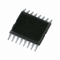
SC18IS600IPW,112 NXP Semiconductors, SC18IS600IPW,112 Datasheet - Page 9

SC18IS600IPW,112
Manufacturer Part Number
SC18IS600IPW,112
Description
IC INTERFACE SPI/I2C 16-TSSOP
Manufacturer
NXP Semiconductors
Datasheet
1.SC18IS600IBS151.pdf
(30 pages)
Specifications of SC18IS600IPW,112
Package / Case
16-TSSOP
Controller Type
I²C Bus Controller
Interface
SPI
Voltage - Supply
2.4 V ~ 3.6 V
Current - Supply
11mA
Operating Temperature
-40°C ~ 85°C
Mounting Type
Surface Mount
Maximum Operating Temperature
+ 125 C
Minimum Operating Temperature
- 55 C
Mounting Style
SMD/SMT
Lead Free Status / RoHS Status
Lead free / RoHS Compliant
For Use With
568-3511 - DEMO BOARD SPI TO I2C
Lead Free Status / Rohs Status
Lead free / RoHS Compliant
Other names
568-3232-5
935279912112
SC18IS600IPW
935279912112
SC18IS600IPW
Available stocks
Company
Part Number
Manufacturer
Quantity
Price
Company:
Part Number:
SC18IS600IPW,112
Manufacturer:
TI
Quantity:
203
NXP Semiconductors
SC18IS600_601_5
Product data sheet
6.2.2 I/O pins state register (IOState)
6.2.3 I
6.2.4 I
When read, this register returns the actual state of all programmable and
quasi-bidirectional I/O pins. When written, each register bit will be transferred to the
corresponding I/O pin programmed as output.
Table 5.
The contents of the register represents the device’s own I
significant bit corresponds to the first bit received from the I
condition. The least significant bit is not used, but should be programmed with a ‘0’.
I2CAdr is not needed for device operation, but should be configured so that its address
does not conflict with an I
This register determines the I
Table 6
I
Bit
7:6
5
4
3
2
1
0
2
2
2
Fig 9.
C-bus address register (I2CAdr)
C-bus clock rates register (I2CClk)
C-bus clock frequency
for the SC18IS600. The frequency can be determined using
Push-pull output configuration
Symbol
-
IO5
IO4
GPIO3 (SC18IS600 only)
GPIO2
GPIO1
GPIO0
IOState - I/O pins state register (address 0x01) bit description
pin latch data
Rev. 05 — 28 July 2008
2
C-bus device address used by the bus master.
=
input data
7.3728 10
------------------------------ - Hz
2
4
C-bus clock frequency. Various clock rates are shown in
I 2CClk
Description
reserved
Set the logic level on the output pins.
Write to this register:
A read from this register returns states of all pins.
logic 0 = set output pin to zero
logic 1 = set output pin to one
6
N
P
V
SS
glitch rejection
strong
V
DD
2
SC18IS600/601
C-bus address. The most
2
002aab885
C-bus after a START
GPIO pin
SPI to I
Equation
© NXP B.V. 2008. All rights reserved.
2
C-bus interface
1:
9 of 30
(1)


