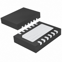
LTC4264IDE#PBF Linear Technology, LTC4264IDE#PBF Datasheet - Page 19

LTC4264IDE#PBF
Manufacturer Part Number
LTC4264IDE#PBF
Description
IC CNTRLR PD INTERFACE 12-DFN
Manufacturer
Linear Technology
Datasheet
1.LTC4264CDEPBF.pdf
(24 pages)
Specifications of LTC4264IDE#PBF
Controller Type
Power over Ethernet Controller (POE)
Interface
IEEE 802.3af
Current - Supply
3mA
Operating Temperature
-40°C ~ 85°C
Mounting Type
Surface Mount
Package / Case
12-DFN
Lead Free Status / RoHS Status
Lead free / RoHS Compliant
Voltage - Supply
-
Available stocks
Company
Part Number
Manufacturer
Quantity
Price
R
the value of R
I
sifi cation given in the electrical specifi cations. The R
resistor must be 1% or better to avoid degrading the overall
accuracy of the classifi cation circuit. Resistor power dissi-
pation will be 100mW maximum and is transient so heating
is typically not a concern. In order to maintain loop stabil-
ity, the layout should minimize capacitance at the R
node. The classifi cation circuit can be disabled by fl oating
the R
V
to attempt to source very large currents. In this case, the
LTC4264 will quickly go into thermal shutdown.
APPLICATIONS INFORMATION
IN_CLASS
IN
CLASS
R
as this would force the LTC4264 classifi cation circuit
CLASS
CLASS
from Table 2. If a unique load current is required,
is the LTC4264 IC supply current during clas-
= 1.237V/(I
pin. The R
CLASS
can be calculated as:
LOAD
CLASS
– I
pin should not be shorted to
IN_CLASS
PSE
PSE
PSE
TO
TO
TO
–54V
–54V
–54V
)
Figure 11. Power Good Interface Examples
V
V
V
IN
IN
IN
LTC4264
LTC4264
LTC4264
ACTIVE-HIGH ENABLE
PWRGD
PWRGD
PWRGD
ACTIVE-LOW ENABLE
CLASS
CLASS
V
V
V
GND
GND
GND
OUT
OUT
OUT
ACTIVE-LOW ENABLE
MMBZ5231B
MMBD4148
Power Good Interface
The LTC4264 provides complimentary power good signals
to simplify the DC/DC converter interface. Using the power
good signal to delay converter operation until the load
capacitor is fully charged is recommended as this will help
ensure trouble free start up. The active high PWRGD pin
is controlled by an open collector transistor referenced to
V
high voltage, open-drain MOSFET referenced to V
designer has the option of using either of these signals to
enable the DC/DC converter and example interface circuits
are shown in Figure 11. When using PWRGD, diode D9
and resistor R
excessive reverse voltage.
5.1V
OUT
R9
100k
R10
100k
10k
10k
D9
R
R
D9
RUN
S
S
LOAD
PD
while the active low PWRGD pin is controlled by a
SHDN
LOAD
Q1
FMMT2222
PD
S
protects the converter shutdown pin from
4264 F11
LOAD
PD
V
+
LTC4264
19
IN
. The
4264f


