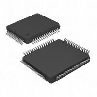
KSZ8873FLLI Micrel Inc, KSZ8873FLLI Datasheet - Page 31

KSZ8873FLLI
Manufacturer Part Number
KSZ8873FLLI
Description
IC ETHERNET SWITCH 3PORT 64LQFP
Manufacturer
Micrel Inc
Specifications of KSZ8873FLLI
Controller Type
Ethernet Switch Controller
Interface
MII
Voltage - Supply
1.8V, 2.5V, 3.3V
Operating Temperature
-40°C ~ 85°C
Mounting Type
Surface Mount
Package / Case
64-LQFP
Lead Free Status / RoHS Status
Lead free / RoHS Compliant
Current - Supply
-
Lead Free Status / Rohs Status
Supplier Unconfirmed
Other names
576-3632
KSZ8873FLLI
KSZ8873FLLI
Available stocks
Company
Part Number
Manufacturer
Quantity
Price
Micrel, Inc.
MII Management (MIIM) Interface
The KSZ8873MLL/FLL/RLL supports the IEEE 802.3 MII Management Interface, also known as the Management Data
Input/Output (MDIO) Interface. This interface allows upper-layer devices to monitor and control the states of the
KSZ8873MLL/FLL/RLL. An external device with MDC/MDIO capability is used to read the PHY status or configure the
PHY settings. Further detail on the MIIM interface is found in Clause 22.2.4.5 of the IEEE 802.3u Specification and refer
to 802.3 section 22.3.4 for the timing.
The MIIM interface consists of the following:
The MIIM Interface can operate up to a maximum clock speed of 5MHz.
The following table depicts the MII Management Interface frame format.
Serial Management Interface (SMI)
The SMI is the KSZ8873MLL/FLL/RLL non-standard MIIM interface that provides access to all KSZ8873MLL/FLL/RLL
configuration registers. This interface allows an external device to completely monitor and control the states of the
KSZ8873MLL/FLL/RLL.
The SMI interface consists of the following:
The following table depicts the SMI frame format.
SMI register read access is selected when OP Code is set to “00” and bit 4 of the PHY address is set to ‘1’. SMI register
write access is selected when OP Code is set to “00” and bit 4 of the PHY address is set to ‘0’. PHY address bit[3] is
undefined for SMI register access, and hence can be set to either ‘0’ or ‘1’ in read/write operations.
To access the KSZ8873MLL/FLL/RLL registers 0-196 (0x00 – 0xC6), the following applies:
September 2010
Read
Write
Read
Write
PHYAD[2:0] and REGAD[4:0] are concatenated to form the 8-bit address;
that is, {PHYAD[2:0], REGAD[4:0]} = bits [7:0] of the 8-bit address.
A physical connection that incorporates the data line (SDA_MDIO) and the clock line (SCL_MDC).
A specific protocol that operates across the aforementioned physical connection that allows an external
Access to a set of eight 16-bit registers, consisting of six standard MIIM registers [0:5] and two custom MIIM
A physical connection that incorporates the data line (SDA_MDIO) and the clock line (SCL_MDC).
A specific protocol that operates across the aforementioned physical connection that allows an external
controller to communicate with the KSZ8873MLL/FLL/RLL device.
Access to all KSZ8873MLL/FLL/RLL configuration registers. Register access includes the Global, Port and
Advanced Control Registers 0-198 (0x00 – 0xC6), and indirect access to the standard MIIM registers [0:5] and
custom MIIM registers [29, 31].
controller to communicate with the KSZ8873MLL/FLL/RLL device.
registers [29, 31].
Preamble
Preamble
32 1’s
32 1’s
32 1’s
32 1’s
Start of
Start of
Frame
Frame
01
01
01
01
Table 9. Serial Management Interface (SMI) Frame Format
Table 8. MII Management Interface Frame Format
Read/Write
Read/Write
OP Code
OP Code
00
00
10
01
Bits [4:0]
Bits [4:0]
Address
Address
AAAAA
AAAAA
1xRRR
0xRRR
PHY
PHY
31
Bits [4:0]
Bits [4:0]
Address
Address
RRRRR
RRRRR
RRRRR
RRRRR
REG
REG
TA
TA
Z0
10
Z0
10
Data Bits [15:0]
0000_0000_DDDD_DDDD
xxxx_xxxx_DDDD_DDDD
Data Bits [15:0]
DDDDDDDD_DDDDDDDD
DDDDDDDD_DDDDDDDD
KSZ8873MLL/FLL/RLL
M9999-092309-1.2
Idle
Idle
Z
Z
Z
Z


