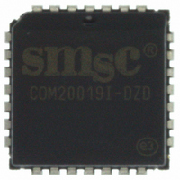
COM20019I-DZD SMSC, COM20019I-DZD Datasheet - Page 33

COM20019I-DZD
Manufacturer Part Number
COM20019I-DZD
Description
IC CTRLR ARCNET 2KX8 RAM 28-PLCC
Manufacturer
SMSC
Series
ARCNETr
Datasheet
1.COM20019I-DZD.pdf
(65 pages)
Specifications of COM20019I-DZD
Controller Type
ARCNET Controller
Interface
Differential
Voltage - Supply
4.5 V ~ 5.5 V
Current - Supply
20mA
Operating Temperature
0°C ~ 70°C
Mounting Type
Surface Mount
Package / Case
28-PLCC
Lead Free Status / RoHS Status
Lead free / RoHS Compliant
Other names
638-1000-5
Available stocks
Company
Part Number
Manufacturer
Quantity
Price
Company:
Part Number:
COM20019I-DZD
Manufacturer:
SMSC
Quantity:
1 028
Company:
Part Number:
COM20019I-DZD
Manufacturer:
Microchip Technology
Quantity:
10 000
Company:
Part Number:
COM20019I-DZD-TR
Manufacturer:
Microchip Technology
Quantity:
10 000
SMSC COM20019I
Cost Competitive ARCNET (ANSI 878.1) Controller with 2K x 8 On-Chip RAM
3,2,1 Clock Prescaler
0
7
6,5,4
3
2
1,0
BIT
BIT
Bits 3,2,1
Slow Arbitration
Select
Read Bus Timing
Select
Reserved
Enhanced
Functions
No Synchronous
Reconfiguration
Timer 1, 0
BIT NAME
BIT NAME
CKP3,2,1
SLOWARB
RBUSTMG This bit is used to Disable/Enable the High Speed CPU
EF
NOSYNC
RCNTM1,
0
SYMBOL
SYMBOL
Table 6.11 - Setup 2 Register
DATASHEET
Read function for High Speed CPU bus support.
RBUSTMG=0: Disable (Default), RBUSTMG=1: Enable. It
does not influence write operation. High speed CPU Read
operation is only for non-multiplexed bus.
These bits are undefined.
This bit is used to enable the new enhanced functions in the
COM20019I. EF = 0: Disable (Default), EF = 1: Enable. If
EF = 0, the timing and function is the same as in the
COM20020, Revision B. See appendix “A”. EF bit must be
‘1’ if the data rate is over 5Mbps.
EF bit should be ‘1’ for new design customers.
EF bit should be ‘0’ for replacement customers.
This bit is used to enable the SYNC command during
initialization. NOSYNC= 0, Enable (Default) The line must
be idle for the RAM initialization sequence to be written.
NOSYNC= 1, Disable:) The line does not have to be idle for
the RAM initialization sequence to be written. See appendix
“A”.
These bits are used to program the reconfiguration timer as
a function of maximum node count. These bits set the time
out period of the reconfiguration timer as shown below. The
time out periods shown are for 312.5 Kbps.
RCNTM1
0
0
1
1
Note*: The node ID value 255 must exist in the network for
420 mS timeout to be valid.
These bits are used to determine the data rate of the
COM20019I. The following table is for a 20 MHz crystal:
CKP3
0
1
Note: The lowest data rate achievable by the COM20019I
is 156.25 Kbs. Defaults to 011 or 312.5 Kbps.
This bit, when set, will divide the arbitration clock by 2.
Memory cycle times will increase when slow arbitration is
selected.
Defaults to low.
Page 33
CKP2
1
0
RCNTM0
0
1
0
1
CKP1
1
0
DESCRIPTION
DESCRIPTION
Time Out
Period
6.72 S
1.68 S
840 mS
420 mS*
DIVISOR
64
128
SPEED
312.5 Kbs
156.25 Kbs
Max Node Count
Up to 255 nodes
Up to 64 nodes
Up to 32 nodes
Up to 16 nodes
Rev. 09-25-07


