CY7C63833-LTXC Cypress Semiconductor Corp, CY7C63833-LTXC Datasheet - Page 52
CY7C63833-LTXC
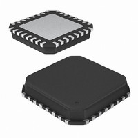
Manufacturer Part Number
CY7C63833-LTXC
Description
IC USB PERIPHERAL CTRLR 32VQFN
Manufacturer
Cypress Semiconductor Corp
Series
CY7Cr
Type
USB Peripheral Controllerr
Datasheet
1.CY7C63310-SXC.pdf
(86 pages)
Specifications of CY7C63833-LTXC
Package / Case
32-VQFN Exposed Pad, 32-HVQFN, 32-SQFN, 32-DHVQFN
Controller Type
USB Peripheral Controller
Interface
USB
Voltage - Supply
4 V ~ 5.5 V
Current - Supply
40mA
Operating Temperature
0°C ~ 70°C
Mounting Type
Surface Mount
Mounting Style
SMD/SMT
Operating Temperature Range
0 C to + 70 C
Supply Current
40 mA
Operating Supply Voltage
4 V to 5.5 V
Lead Free Status / RoHS Status
Lead free / RoHS Compliant
For Use With
770-1001 - ISP 4PORT CYPRESS ENCORE II MCUCY4623 - KIT MOUSE REFERENCE DESIGN428-1774 - EXTENSION KIT FOR ENCORE II428-1773 - KIT DEVELOPMENT ENCORE II
Lead Free Status / Rohs Status
Lead free / RoHS Compliant
Available stocks
Company
Part Number
Manufacturer
Quantity
Price
Company:

Part Number:
CY7C63833-LTXC
Manufacturer:
Cypress
Quantity:
2 814
Part Number:
CY7C63833-LTXC
Manufacturer:
CYPRESS/赛普拉斯
Quantity:
20 000


17.2 Interrupt Processing
The sequence of events that occur during interrupt processing
follows:
Document 38-08035 Rev. *N
1. An interrupt becomes active, because:
1. The current executing instruction finishes.
2. The internal interrupt is dispatched, taking 13 cycles. During
1. Program execution vectors to the interrupt table. Typically, a
2. The ISR executes. Note that interrupts are disabled because
a. The interrupt condition occurs (for example, a timer expires).
b. A previously posted interrupt is enabled through an update
c. An interrupt is pending and GIE is set from 0 to 1 in the CPU
a. The PCH, PCL, and Flag register (CPU_F) are stored onto
b. The CPU_F register is then cleared. Because this clears the
c. The PCH (PC[15:8]) is cleared to zero.
d. The interrupt vector is read from the interrupt controller and
this time, the following actions occur: the MSB and LSB of
Program Counter and Flag registers (CPU_PC and CPU_F)
are stored onto the program stack by an automatic CALL
instruction (13 cycles) generated during the interrupt
acknowledge process.
LJMP instruction in the interrupt table sends execution to the
user's Interrupt Service Routine (ISR) for this interrupt.
GIE = 0. In the ISR, interrupts are re-enabled by setting
GIE = 1 (care must be taken to avoid stack overflow).
of an interrupt mask register.
Flag register.
the program stack (in that order) by an automatic CALL
instruction (13 cycles) generated during the interrupt
acknowledge process
GIE bit to 0, additional interrupts are temporarily disabled.
its value placed into PCL (PC[7:0]). This sets the program
counter to point to the appropriate address in the interrupt
table (for example, 0004h for the POR/LVD interrupt).
GPIO, etc.)
Interrupt
Source
(Timer,
1
INT_CLRx Write
Interrupt Taken
D
or
R
Q
Figure 17-1. Interrupt Controller Block Diagram
Mask Bit Setting
Interrupt
INT_MSKx
Posted
Interrupt
Pending
17.3 Interrupt Trigger Conditions
Trigger conditions for most interrupts in
have been explained in the relevant sections. However,
conditions under which the USB Active (interrupt address 0030h)
and PS2 Data Low (interrupt address 004Ch) interrupts are
triggered are explained follow.
17.4 Interrupt Latency
The time between the assertion of an enabled interrupt and the
start of its ISR is calculated from the following equation.
Latency = Time for current instruction to finish + Time for internal
interrupt routine to execute + Time for LJMP instruction in
interrupt table to execute.
For example, if the 5 cycle JMP instruction is executing when an
interrupt becomes active, the total number of CPU clock cycles
before the ISR begins is as follows:
(1 to 5 cycles for JMP to finish) + (13 cycles for interrupt routine)
+ (7 cycles for LJMP) = 21 to 25 cycles.
In the previous example, at 24 MHz, 25 clock cycles take
1.042 μs.
3. The ISR ends with a RETI instruction which restores the
4. Execution resumes at the next instruction, after the one that
1. USB Active Interrupt: Triggered when the D+/- lines are in a
2. PS2 Data Low Interrupt: Triggered when SDATA becomes low
3. The GPIO interrupts are edge triggered.
Program Counter and Flag registers (CPU_PC and CPU_F).
The restored Flag register re-enables interrupts, because
GIE = 1 again.
occurred before the interrupt. However, if there are more
pending interrupts, the subsequent interrupts are processed
before the next normal program instruction.
non-idle state, that is, K-state or SE0 state.
when the SDATA pad is in the input mode for at least 6-7
32 kHz cycles.
Encoder
Priority
CPU_F[0]
Interrupt Vector
CY7C63310, CY7C638xx
GIE
Interrupt
Request
Table 17-1 on page 51
M8C Core
Page 52 of 86
[+] Feedback
Related parts for CY7C63833-LTXC
Image
Part Number
Description
Manufacturer
Datasheet
Request
R

Part Number:
Description:
IC USB PERIPHERAL CTRLR 32VQFN
Manufacturer:
Cypress Semiconductor Corp
Datasheet:

Part Number:
Description:
CY7C63833-LTXCT
Manufacturer:
Cypress Semiconductor Corp
Datasheet:
Part Number:
Description:
Manufacturer:
Cypress Semiconductor Corp
Datasheet:
Part Number:
Description:
Manufacturer:
Cypress Semiconductor Corp
Datasheet:
Part Number:
Description:
Manufacturer:
Cypress Semiconductor Corp
Datasheet:
Part Number:
Description:
Manufacturer:
Cypress Semiconductor Corp
Datasheet:
Part Number:
Description:
Manufacturer:
Cypress Semiconductor Corp
Datasheet: