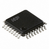
TDA8029HL/C207,118 NXP Semiconductors, TDA8029HL/C207,118 Datasheet - Page 44

TDA8029HL/C207,118
Manufacturer Part Number
TDA8029HL/C207,118
Description
IC SMART CARD READER 32-LQFP
Manufacturer
NXP Semiconductors
Datasheet
1.TDA8029HLC207118.pdf
(59 pages)
Specifications of TDA8029HL/C207,118
Package / Case
32-LQFP
Controller Type
Smart Card Reader Interface
Interface
Serial
Voltage - Supply
2.7 V ~ 6 V
Current - Supply
250mA
Operating Temperature
-40°C ~ 90°C
Mounting Type
Surface Mount
Maximum Operating Temperature
+ 90 C
Minimum Operating Temperature
- 40 C
Mounting Style
SMD/SMT
Lead Free Status / RoHS Status
Lead free / RoHS Compliant
Lead Free Status / RoHS Status
Lead free / RoHS Compliant, Lead free / RoHS Compliant
Other names
568-2233-2
935274733118
TDA8029HL07BD-T
935274733118
TDA8029HL07BD-T
Available stocks
Company
Part Number
Manufacturer
Quantity
Price
Company:
Part Number:
TDA8029HL/C207,118
Manufacturer:
NXP Semiconductors
Quantity:
10 000
Part Number:
TDA8029HL/C207,118
Manufacturer:
NXP/恩智浦
Quantity:
20 000
Philips Semiconductors
9397 750 14145
Product data sheet
8.17 Deactivation sequence
When everything is satisfactory (voltage supply, card present and no hardware problems),
the system controller may initiate an activation sequence of the card.
activation sequence.
After leaving the UART reset mode, and then configuring the necessary parameters for
the UART, it may set the bit START in register PCR (t
place:
After a number of clock pulses that can be counted with the time-out counter, bit RSTIN
may be set by software, then pin RST rises to V
The sequencer is clocked by
t
When the session is completed, the microcontroller resets bit START (t
executes an automatic deactivation sequence shown in
1
Fig 12. Activation sequence
•
•
•
•
•
•
•
•
•
= 0 to
The DC-to-DC converter is started (t
V
typically (t
I/O rises to V
CLK is sent to the card and RST is enabled (t
START
Card reset (pin RST falls LOW) (t
Clock (pin CLK) is stopped LOW (t
Pin I/O falls to 0 V (t
V
The DC-to-DC converter is stopped and CLK, RST, V
low-impedance to GNDC (t
RSTIN
CC
CC
RST
V
CLK
V
I/O
UP
CC
3
starts rising from 0 V to 5 V or 3 V with a controlled rise time of 0.17 V/ s
falls to 0 V with typical 0.17 V/ s slew rate (t
64
T, t
2
2
)
= t
CC
t
0
1
t
1
(t
+
Rev. 03 — 22 February 2005
3
3
), (Integrated 14 k pull-up to V
2
13
t
T, t
2
)
3
1
= t
64
15
1
f
int
).
+
7
which leads to a time interval T of 25 s typical. Thus
2
t
11
3
T, and t
12
)
1
)
t
)
4
= t
act
4
= t
CC
1
4
.
).
+ 4T.
14
0
). The following sequence will take
CC
)
Figure
)
CC
Low power single card reader
© Koninklijke Philips Electronics N.V. 2005. All rights reserved.
and I/O become
13:
Figure 12
10
TDA8029
). The circuit then
shows the
ATR
fce684
44 of 59


