UDA1380TT/N2,512 NXP Semiconductors, UDA1380TT/N2,512 Datasheet - Page 23
UDA1380TT/N2,512
Manufacturer Part Number
UDA1380TT/N2,512
Description
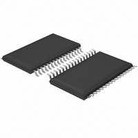
IC AUDIO CODER-DECODER 32-TSSOP
Manufacturer
NXP Semiconductors
Type
Stereo Audior
Datasheet
1.UDA1380HNN2118.pdf
(68 pages)
Specifications of UDA1380TT/N2,512
Package / Case
32-TSSOP
Data Interface
I²C, Serial
Resolution (bits)
24 b
Number Of Adcs / Dacs
2 / 2
Sigma Delta
No
S/n Ratio, Adcs / Dacs (db) Typ
97 / 100
Voltage - Supply, Analog
2.4 V ~ 3.6 V
Voltage - Supply, Digital
2.4 V ~ 3.6 V
Operating Temperature
-40°C ~ 85°C
Mounting Type
Surface Mount
Interface Type
Serial (I2C)
Resolution
24 bit
Operating Supply Voltage
3 V
Maximum Operating Temperature
+ 85 C
Mounting Style
SMD/SMT
Minimum Operating Temperature
- 40 C
Supply Current
10 mA
Thd Plus Noise
- 85 dB
Lead Free Status / RoHS Status
Lead free / RoHS Compliant
Other names
935270659512
UDA1380TT
UDA1380TT
UDA1380TT
UDA1380TT


NXP Semiconductors
9.5
For writing data to a device, four bytes must be sent. Figure 14 explains the data write mode in a signal diagram:
• One byte with the device address, being ‘00000110’, which is including the LSB code 01 for signalling write to the
• One byte starting with a logic 0 for signalling write, followed by 7 bits indicating the destination address
• Two data bytes.
Table 8 L3 write data
Notes
1. First bit in time.
2. Last bit in time.
9.6
For reading from the device, first a prepare-read must be
done. After this, the device address is sent again. The
device then returns with the register address, indicating
whether the address was valid or not, and the data of the
register. The following five steps explain this procedure,
and an example of transmission is given in Fig.15.
• One byte with the device address, being ‘00000110’,
• One byte is sent with the register address from which it
2004 Apr 22
The SYSCLK signal must be applied in data write mode.
Addressing mode
Data transfer 1
Data transfer 2
Data transfer 3
device
which is including the LSB code 01 for signalling write to
the device
needs to be read. This byte starts with a logic 1, which
indicates that there will be a read action from the register
Stereo audio coder-decoder
for MD, CD and MP3
L3 MODE
Data write mode
Data read mode
device address
register address
MS data byte
LS data byte
DATA TYPE
D15
0
D7
0
0
(1)
D14
D6
A6
1
1
23
• One byte with the device address including ‘11’ is sent
• The device now writes the requested register address
• The device writes the data from the requested register
The SYSCLK signal must be applied in data read mode.
D13
D5
A5
to the device, being 00000111. The ‘11’ indicates that
the device must write data to the microcontroller, then
the microcontroller frees the L3DATA-bus so the
UDA1380 can send the register address byte and its
two-byte contents
on the bus, indicating whether the requested register
was valid or not (logic 0 means valid, logic 1 means
invalid)
on the bus, being two bytes.
2
1
D12
D4
A4
3
0
BIT
D11
D3
A3
4
0
D10
D2
A2
5
0
Product specification
UDA1380
D9
D1
A1
6
0
7
A0
D8
D0
0
(2)
Related parts for UDA1380TT/N2,512
Image
Part Number
Description
Manufacturer
Datasheet
Request
R

Part Number:
Description:
Audio CODECs SSA CODEC
Manufacturer:
NXP Semiconductors
Datasheet:

Part Number:
Description:
IC AUDIO CODER-DECODER 32-TSSOP
Manufacturer:
NXP Semiconductors
Datasheet:
Part Number:
Description:
Uda1380 Stereo Audio Coder-decoder For Md, Cd And Mp3
Manufacturer:
NXP Semiconductors
Datasheet:

Part Number:
Description:
UDA1380; Stereo Audio Coder-decoder For MD, CD And MP3
Manufacturer:
Philips Semiconductors (Acquired by NXP)
Datasheet:
Part Number:
Description:
NXP Semiconductors designed the LPC2420/2460 microcontroller around a 16-bit/32-bitARM7TDMI-S CPU core with real-time debug interfaces that include both JTAG andembedded trace
Manufacturer:
NXP Semiconductors
Datasheet:

Part Number:
Description:
NXP Semiconductors designed the LPC2458 microcontroller around a 16-bit/32-bitARM7TDMI-S CPU core with real-time debug interfaces that include both JTAG andembedded trace
Manufacturer:
NXP Semiconductors
Datasheet:
Part Number:
Description:
NXP Semiconductors designed the LPC2468 microcontroller around a 16-bit/32-bitARM7TDMI-S CPU core with real-time debug interfaces that include both JTAG andembedded trace
Manufacturer:
NXP Semiconductors
Datasheet:
Part Number:
Description:
NXP Semiconductors designed the LPC2470 microcontroller, powered by theARM7TDMI-S core, to be a highly integrated microcontroller for a wide range ofapplications that require advanced communications and high quality graphic displays
Manufacturer:
NXP Semiconductors
Datasheet:
Part Number:
Description:
NXP Semiconductors designed the LPC2478 microcontroller, powered by theARM7TDMI-S core, to be a highly integrated microcontroller for a wide range ofapplications that require advanced communications and high quality graphic displays
Manufacturer:
NXP Semiconductors
Datasheet:
Part Number:
Description:
The Philips Semiconductors XA (eXtended Architecture) family of 16-bit single-chip microcontrollers is powerful enough to easily handle the requirements of high performance embedded applications, yet inexpensive enough to compete in the market for hi
Manufacturer:
NXP Semiconductors
Datasheet:
Part Number:
Description:
The XA-S3 device is a member of Philips Semiconductors? XA(eXtended Architecture) family of high performance 16-bitsingle-chip microcontrollers
Manufacturer:
NXP Semiconductors
Datasheet:

Part Number:
Description:
The NXP BlueStreak LH75401/LH75411 family consists of two low-cost 16/32-bit System-on-Chip (SoC) devices
Manufacturer:
NXP Semiconductors
Datasheet:
Part Number:
Description:
The NXP LPC3130/3131 combine an 180 MHz ARM926EJ-S CPU core, high-speed USB2
Manufacturer:
NXP Semiconductors
Datasheet: