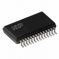
UDA1342TS/N1,512 NXP Semiconductors, UDA1342TS/N1,512 Datasheet - Page 35

UDA1342TS/N1,512
Manufacturer Part Number
UDA1342TS/N1,512
Description
IC AUDIO CODEC MINIDISC 28-SSOP
Manufacturer
NXP Semiconductors
Type
Stereo Audior
Datasheet
1.UDA1342TSN1518.pdf
(45 pages)
Specifications of UDA1342TS/N1,512
Package / Case
28-SSOP (0.200", 5.30mm Width)
Data Interface
Serial
Resolution (bits)
24 b
Number Of Adcs / Dacs
4 / 2
Sigma Delta
No
S/n Ratio, Adcs / Dacs (db) Typ
99 / 99
Voltage - Supply, Analog
2.7 V ~ 3.6 V
Voltage - Supply, Digital
2.7 V ~ 3.6 V
Operating Temperature
-40°C ~ 85°C
Mounting Type
Surface Mount
Number Of Adc Inputs
4
Number Of Dac Outputs
2
Conversion Rate
110 KSPs
Interface Type
Serial (I2C), L3
Resolution
24 bit
Operating Supply Voltage
2.7 V to 3.6 V
Maximum Operating Temperature
+ 85 C
Mounting Style
SMD/SMT
Minimum Operating Temperature
- 40 C
Number Of Channels
4 ADC, 2 DAC
Supply Current
20 mA
Lead Free Status / RoHS Status
Lead free / RoHS Compliant
Other names
568-1155-5
935262909512
UDA1342TSDB
935262909512
UDA1342TSDB
NXP Semiconductors
Notes
1. The typical value of the timing is specified at 48 kHz sampling frequency.
2. In order to prevent digital noise interfering with the L3-bus communication, it is best to have the rise and fall times as
3. When the sampling frequency is below 32 kHz, the L3CLOCK cycle must be limited to
4. C
5. After this period, the first clock pulse is generated.
6. To be suppressed by the input filter.
2000 Jul 31
t
t
t
t
t
t
t
t
t
I
f
t
t
t
t
t
t
t
t
t
t
t
C
su(L3)D
h(L3)D
stp(L3)
su(L3)DA
h(L3)DA
su(L3)R
h(L3)R
en(L3)R
dis(L3)R
2
SCL
LOW
HIGH
r
f
HD;STA
SU;STA
SU;STO
BUF
SU;DAT
HD;DAT
SP
C-bus interface timing (see Fig.15)
Audio CODEC
b
SYMBOL
SYMBOL
small as possible.
b
is the total capacitance of one bus line in pF. The maximum capacitive load for each bus line is 400 pF.
L3MODE set-up time in data
transfer mode
L3MODE hold time in data
transfer mode
L3MODE stop time in data
transfer mode
L3DATA set-up time in address
and data transfer mode
L3DATA hold time in address and
data transfer mode
L3DATA set-up time for read data
L3DATA hold time for read data
L3DATA enable time for read data
L3DATA disable time for read
data
SCL clock frequency
SCL LOW time
SCL HIGH time
rise time SDA and SCL
fall time SDA and SCL
hold time START condition
set-up time repeated START
set-up time STOP condition
bus free time between a STOP
and START condition
data set-up time
data hold time
pulse width of spikes
capacitive load for each bus line
PARAMETER
PARAMETER
note 4
note 4
note 6
note 5
CONDITIONS
CONDITIONS
35
190
190
190
190
30
50
360
380
50
0
1.3
0.6
20 + 0.1C
20 + 0.1C
0.6
0.6
0.6
1.3
100
0
0
−
MIN.
MIN.
b
b
−
−
−
−
−
−
−
−
−
−
−
−
−
−
−
−
−
−
−
−
−
−
TYP.
TYP.
1
⁄
64fs
cycle.
UDA1342TS
−
−
−
−
−
−
−
−
−
400
−
−
300
300
−
−
−
−
−
−
50
400
Product specification
MAX.
MAX.
ns
ns
ns
ns
ns
ns
ns
ns
ns
kHz
μs
μs
ns
ns
μs
μs
μs
μs
ns
μs
ns
pF
UNIT
UNIT


