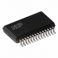
UDA1342TS/N1,512 NXP Semiconductors, UDA1342TS/N1,512 Datasheet - Page 18

UDA1342TS/N1,512
Manufacturer Part Number
UDA1342TS/N1,512
Description
IC AUDIO CODEC MINIDISC 28-SSOP
Manufacturer
NXP Semiconductors
Type
Stereo Audior
Datasheet
1.UDA1342TSN1518.pdf
(45 pages)
Specifications of UDA1342TS/N1,512
Package / Case
28-SSOP (0.200", 5.30mm Width)
Data Interface
Serial
Resolution (bits)
24 b
Number Of Adcs / Dacs
4 / 2
Sigma Delta
No
S/n Ratio, Adcs / Dacs (db) Typ
99 / 99
Voltage - Supply, Analog
2.7 V ~ 3.6 V
Voltage - Supply, Digital
2.7 V ~ 3.6 V
Operating Temperature
-40°C ~ 85°C
Mounting Type
Surface Mount
Number Of Adc Inputs
4
Number Of Dac Outputs
2
Conversion Rate
110 KSPs
Interface Type
Serial (I2C), L3
Resolution
24 bit
Operating Supply Voltage
2.7 V to 3.6 V
Maximum Operating Temperature
+ 85 C
Mounting Style
SMD/SMT
Minimum Operating Temperature
- 40 C
Number Of Channels
4 ADC, 2 DAC
Supply Current
20 mA
Lead Free Status / RoHS Status
Lead free / RoHS Compliant
Other names
568-1155-5
935262909512
UDA1342TSDB
935262909512
UDA1342TSDB
NXP Semiconductors
8.16
Besides the L3-bus mode the UDA1342TS supports the
I
microcontroller with the same register addresses as used
in the L3-bus mode.
The exchange of data and control information between the
microcontroller and the UDA1342TS in the I
is accomplished through a serial hardware interface
comprising the following pins and signals:
• L3CLOCK: Serial Clock Line (SCL)
• L3DATA: Serial Data line (SDA).
The clock and data timing of the I
in Fig.15.
8.16.1
Before any data is transmitted on the I
which should respond is addressed first. The addressing is
always done with the first byte transmitted after the START
procedure (S).
8.16.2
The UDA1342TS acts as a slave receiver or a slave
transmitter. Therefore, the clock signal SCL is only an
input signal. The data signal SDA is an input or output
signal (bidirectional line).
The UDA1342TS slave address format is shown in
Table 15.
Table 15 I
The slave address bit IPSEL corresponds to the hardware
address pin IPSEL which allows selecting the slave
address.
2000 Jul 31
2
MSB BIT 6 BIT 5 BIT 4 BIT 3 BIT 2 BIT 1 LSB
C-bus mode; all the features can be controlled by the
Audio CODEC
0
I
2
C-bus interface
A
S
0
DDRESSING
LAVE ADDRESS
2
C-bus slave address format
1
1
0
2
C-bus transfer is shown
2
C-bus, the device
1
2
IPSEL R/W
C-bus mode
18
8.16.3
The UDA1342TS register address format is given in
Table 16.
Table 16 I
The register mapping of the I
is the same (see Section 9).
MSB BIT 6 BIT 5 BIT 4 BIT 3 BIT 2 BIT 1 LSB
0
R
A6
2
EGISTER ADDRESS
C-bus register address format
A5
A4
2
C-bus and L3-bus interfaces
A3
UDA1342TS
Product specification
A2
A1
A0


