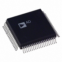
AD1843JS Analog Devices Inc, AD1843JS Datasheet - Page 47

AD1843JS
Manufacturer Part Number
AD1843JS
Description
IC CODEC STEREO 5V 16BIT 80PQFP
Manufacturer
Analog Devices Inc
Type
Stereo Audior
Datasheet
1.AD1843JS.pdf
(64 pages)
Specifications of AD1843JS
Rohs Status
RoHS non-compliant
Data Interface
Serial
Resolution (bits)
16 b
Number Of Adcs / Dacs
1 / 2
Sigma Delta
Yes
S/n Ratio, Adcs / Dacs (db) Typ
92 / 86
Dynamic Range, Adcs / Dacs (db) Typ
85 / 80
Voltage - Supply, Analog
4.75 V ~ 5.25 V
Voltage - Supply, Digital
2.85 V ~ 5.25 V
Operating Temperature
0°C ~ 70°C
Mounting Type
Surface Mount
Package / Case
80-MQFP, 80-PQFP
Available stocks
Company
Part Number
Manufacturer
Quantity
Price
Part Number:
AD1843JS
Manufacturer:
ADI/亚德诺
Quantity:
20 000
REV. 0
DA2SM
DA1SM
DA2F1:0
DA1F1:0
SCF
FRS
FRST
ADTLK
ADRF1:0
ADLF1:0
res
DAC2 Stereo/Mono Mode Select. When in stereo mode, data transmitted to the AD1843 during slot 4 is
used by DAC2 left and data transmitted to the AD1843 during slot 5 is used by DAC2 right. When in
mono mode, data transmitted to the AD1843 during slot 4 is used by both DAC2 left and right, and data
transmitted to the AD1843 during slot 5 is ignored. (Note: slot 0 is assumed to be the first slot.)
0 = Stereo Mode
1 = Mono Mode
DAC1 Stereo/Mono Mode Select. When in stereo mode, data transmitted to the AD1843 during slot 2 is
used by DAC1 left and data transmitted to the AD1843 during slot 3 is used by DAC1 right. When in
mono mode, data transmitted to the AD1843 during slot 2 is used by both DAC1 left and right, and data
transmitted to the AD1843 during slot 3 is ignored. (Note: slot 0 is assumed to be the first slot.)
0 = Stereo Mode
1 = Mono Mode
DAC2 (Left and Right Channels) Data Format Select.
00 = 8-bit Unsigned Linear PCM
01 = 16-bit Signed Linear PCM
10 = 8-bit -Law Companded
11 = 8-bit A-Law Companded
DAC1 (Left and Right Channels) Data Format Select.
00 = 8-bit Unsigned Linear PCM
01 = 16-bit Signed Linear PCM
10 = 8-bit -Law Companded
11 = 8-bit A-Law Companded
SCLK Frequency Select. Changes to this bit do not take effect until shortly after the sixth slot (the final slot
owned) is completed. Relevant when the AD1843 is in Master Mode only.
0 = 12.288 MHz
1 = 16.384 MHz
Frame Size Select. Selects the number of slots per frame. Changes to this bit do not take effect until the
time specified by the FRST bit.
0 = 32 Slots per Frame
1 = 16 Slots per Frame
Frame Size Change Timing. Selects the point in time when FRS takes effect.
0 = Frame Size Changes Once the Current Frame is Complete
1 = Frame Size Changes Immediately, Beginning with the Current Frame
ADC Transmit Lock Mode Select. When this bit is set to “1,” ADC transmit lock mode is entered. In this
mode, left and right ADC samples are transmitted during a frame only if both left and right samples are
ready to be transmitted. When not in ADC transmit lock mode, left and right samples are transmitted as
they individually become available. Note that even if left and right ADCs are programmed to the same
sample rate, unless the AD1843 is in transmit lock mode, ADC samples will not necessarily be transmitted
paired together in a TDM frame. This bit should be set to “1” only if both ADCs are powered down and
only if both ADCs will be programmed to the sample rate once they are enabled. This bit may be reset to
“0” at any time. While in ADC transmit lock mode, both ADCs must be enabled and disabled simulta-
neously (write to Control Register Address 27 must set ADLEN and ADREN both to “0” or to “1”).
0 = ADC Transmit Lock Mode Disabled
1 = ADC Transmit Lock Mode Enabled
ADC Right Channel Data Format Select.
00 = 8-bit Unsigned Linear PCM
01 = 16-bit Signed Linear PCM
10 = 8-bit -Law Companded
11 = 8-bit A-Law Companded
ADC Left Channel Data Format Select.
00 = 8-bit Unsigned Linear PCM
01 = 16-bit Signed Linear PCM
10 = 8-bit -Law Companded
11 = 8-bit A-Law Companded
Reserved for future expansion. To ensure future compatibility, write “0” to all reserved bits.
Initial default state after reset: 0000 0000 0000 0000 (0000 hex). Cleared to default and cannot be written
to when: the RESET pin is asserted LO; or when the PWRDWN pin is asserted LO.
–47–
AD1843


