AD1843JS Analog Devices Inc, AD1843JS Datasheet - Page 45
AD1843JS
Manufacturer Part Number
AD1843JS
Description
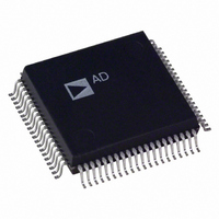
IC CODEC STEREO 5V 16BIT 80PQFP
Manufacturer
Analog Devices Inc
Type
Stereo Audior
Datasheet
1.AD1843JS.pdf
(64 pages)
Specifications of AD1843JS
Rohs Status
RoHS non-compliant
Data Interface
Serial
Resolution (bits)
16 b
Number Of Adcs / Dacs
1 / 2
Sigma Delta
Yes
S/n Ratio, Adcs / Dacs (db) Typ
92 / 86
Dynamic Range, Adcs / Dacs (db) Typ
85 / 80
Voltage - Supply, Analog
4.75 V ~ 5.25 V
Voltage - Supply, Digital
2.85 V ~ 5.25 V
Operating Temperature
0°C ~ 70°C
Mounting Type
Surface Mount
Package / Case
80-MQFP, 80-PQFP
Available stocks
Company
Part Number
Manufacturer
Quantity
Price

Part Number:
AD1843JS
Manufacturer:
ADI/亚德诺
Quantity:
20 000


REV. 0
C3PD
C3P7:0
res
Restrictions: Modem filter should not be selected when channel sample rate is above 24 kHz.
DRSFLT
DAMIX
DA2FLT
Address 24
Address 25
DAADR1
DRSFLT
Data 15
Data 15
Data 7
Data 7
C3P7
res
Clock Generator 3 Phase Shift Direction. This bit controls the direction of sample clock phase shift.
0 = Phase Advance
1 = Phase Retard
Clock Generator 3 Phase Shift Magnitude. These bits control the magnitude of sample clock phase shift. One LSB
represents exactly 0.12 degrees. LSBs are processed and decremented at a rate of 3.072 MHz (assuming a 24.576
MHz clock input on the XTALI pin). When this register is read, it indicates any phase advance/retard remaining to
be processed as of the beginning of slot 0 if bus master, or when TSI was received if bus slave. This register may be
overwritten even if all previously programmed phase advance/retard has not been processed. When written, the con-
tents of this register (just prior to the write) are transmitted during slot 1 of the following frame (as with all Control
Register writes).
Reserved for future expansion. To ensure future compatibility, write “0” to all reserved bits.
Initial default state after reset: 0000 0000 0000 0000 (0000 hex). Cleared to default and cannot be written to when:
the RESET pin is asserted LO; when the PWRDWN pin is asserted LO; or when the G3EN bit in Control Register
Address 28 is reset to “0” (clock generator 3 disabled).
Digital Resampler Filter Mode. DAC2 is sacrificed so that the remaining four channels (left ADC, right ADC, left
and right DAC1) have sufficient resources to realize the more stringent resampling filter requirements. See below for
filter specifications. (Note: Digital resampling can be done without using the resampling filters but performance is not
as optimal.) This bit can be altered only if all channels (DAC1, DAC2, ADL, and ADR) are powered down. Note
that this bit enables the digital resampler filters, but does not enable the digital resampler data pathways. Use the
DAADR1:0 and DAADL1:0 bits to enable the resampler data pathways.
0 = Audio/Modem Filter Modes (Defined by DA1FLT, DA2FLT, ADLFLT and ADRFLT)
1 = Digital Resampler Filter Mode (DA1FLT, DA2FLT, ADLFLT and ADRFLT filter selections are ignored).
DAC Digital Mix Enable. When set to “1,” DAC1 and DAC2 are mixed at the output of the digital interpolation fil-
ter. Left and right channels are still separated, but DAC1 and DAC2 outputs are identical. This bit can be altered
only if both DAC1 and DAC2 are powered down.
0 = Digital Mix Disabled
1 = Digital Mix Enabled
DAC2 (Left and Right Channels) Digital Filter Select and Analog Output Swing Select. Digital filter selected is over-
ridden when DRSFLT is set to “1.” See below for filter specifications. This bit can be altered only if DAC2
is powered down.
0 = Digital Audio Filter. Nominal analog swing is 2.000 V p-p when output level is +0.0 dB (see Control Register
Address 10).
1 = Digital Modem Filter. Nominal analog swing is 3.156 V p-p when output level is +4.5 dB (see Control Register
Address 10).
DAADR0
Data 14
Data 14
DAMIX
Data 6
Data 6
C3P6
res
Clock Generator 3 Control—Sample Phase Shift
Codec Configuration—Digital Filter and Mode Select
DAADL1
Data 13
Data 13
Data 5
Data 5
C3P5
res
res
DAADL0
Data 12
Data 12
Data 4
Data 4
C3P4
res
res
–45–
Data 11
Data 11
Data 3
Data 3
C3P3
res
res
res
Data 10
Data 10
Data 2
Data 2
C3P2
res
res
res
ADRFLT
DA2FLT
Data 9
Data 1
Data 9
Data 1
C3P1
res
ADLFLT
DA1FLT
Data 8
Data 0
C3PD
Data 8
Data 0
C3P0
AD1843
Related parts for AD1843JS
Image
Part Number
Description
Manufacturer
Datasheet
Request
R

Part Number:
Description:
±1.7g Dual-Axis IMEMS Accelerometer Evaluation Board
Manufacturer:
Analog Devices Inc
Datasheet:

Part Number:
Description:
Inertial Sensor Evaluation System
Manufacturer:
Analog Devices Inc
Datasheet:
Part Number:
Description:
Manufacturer:
Analog Devices Inc
Datasheet:
Part Number:
Description:
Manufacturer:
Analog Devices Inc
Datasheet:
Part Number:
Description:
Manufacturer:
Analog Devices Inc
Datasheet:
Part Number:
Description:
Manufacturer:
Analog Devices Inc
Datasheet:
Part Number:
Description:
Manufacturer:
Analog Devices Inc
Datasheet:
Part Number:
Description:
Manufacturer:
Analog Devices Inc
Datasheet:
Part Number:
Description:
Manufacturer:
Analog Devices Inc
Datasheet:
Part Number:
Description:
Manufacturer:
Analog Devices Inc
Datasheet:
Part Number:
Description:
Manufacturer:
Analog Devices Inc
Datasheet:
Part Number:
Description:
Manufacturer:
Analog Devices Inc
Datasheet:
Part Number:
Description:
Manufacturer:
Analog Devices Inc
Datasheet: