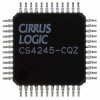
CS4245-CQZ Cirrus Logic Inc, CS4245-CQZ Datasheet - Page 34

CS4245-CQZ
Manufacturer Part Number
CS4245-CQZ
Description
IC CODEC AUD STER 104DB 48LQFP
Manufacturer
Cirrus Logic Inc
Type
Stereo Audior
Datasheet
1.CS4245-CQZ.pdf
(57 pages)
Specifications of CS4245-CQZ
Package / Case
48-LQFP
Data Interface
Serial
Resolution (bits)
24 b
Number Of Adcs / Dacs
2 / 2
Sigma Delta
Yes
Dynamic Range, Adcs / Dacs (db) Typ
104 / 104
Voltage - Supply, Analog
3.13 V ~ 5.25 V
Voltage - Supply, Digital
3.13 V ~ 5.25 V
Operating Temperature
-10°C ~ 70°C
Mounting Type
Surface Mount
Number Of Adc Inputs
12
Number Of Dac Outputs
4
Conversion Rate
192 KSPS
Interface Type
Serial (I2C, SPI)
Resolution
24 bit
Operating Supply Voltage
3.3 V, 5 V
Maximum Operating Temperature
+ 70 C
Mounting Style
SMD/SMT
Minimum Operating Temperature
- 10 C
Number Of Channels
2 ADC/2 DAC
Thd Plus Noise
- 95 dB ADC / - 90 dB DAC
Lead Free Status / RoHS Status
Lead free / RoHS Compliant
For Use With
598-1501 - BOARD EVAL FOR CS4245 CODEC
Lead Free Status / Rohs Status
Lead free / RoHS Compliant
Other names
598-1034
Available stocks
Company
Part Number
Manufacturer
Quantity
Price
Company:
Part Number:
CS4245-CQZ
Manufacturer:
CIRRUS
Quantity:
455
Part Number:
CS4245-CQZ
Manufacturer:
CIRRUS
Quantity:
20 000
Company:
Part Number:
CS4245-CQZR
Manufacturer:
Schneider
Quantity:
1 000
Company:
Part Number:
CS4245-CQZR
Manufacturer:
Cirrus Logic Inc
Quantity:
10 000
34
4.7
4.7.1
4.7.2
4.7.3
4.8
4.9
Output Transient Control
The CS4245 uses Popguard
power-down. This technique eliminates the audio transients commonly produced by single-ended, single-
supply converters when it is implemented with external DC-blocking capacitors connected in series with the
audio outputs. To make best use of this feature, it is necessary to understand its operation.
Auxiliary Analog Output
The CS4245 includes an auxiliary analog output through the AUXOUT pins. These pins can be configured
to output the analog input to the ADC as selected with the input MUX and gained or attenuated with the
PGA, the analog output of the DAC, or alternatively they may be set to high-impedance. See
“Auxiliary Output Source Select (Bits 6:5)” on page
output.
The auxiliary analog output can source very little current. As current from the AUXOUT pins increases, dis-
tortion will increase. For this reason, a high input impedance buffer must be used on the AUXOUT pins to
achieve full performance. Refer to the table in
ceptable loading conditions.
De-Emphasis Filter
The CS4245 includes on-chip digital de-emphasis optimized for a sample rate of 44.1 kHz. The filter re-
sponse is shown in
changes in sample rate, Fs. Please see
phasis control.
The de-emphasis feature is included to accommodate audio recordings that utilize 50/15 μs pre-emphasis
equalization as a means of noise reduction.
Power-Up
When the device is initially powered-up, the audio outputs AOUTA and AOUTB are clamped to VQ2,
which is initially low. After the PDN bit is released (set to ‘0’), the DAC outputs begin to ramp with VQ2
towards the nominal quiescent voltage. This ramp takes approximately 200 ms to complete. The gradual
voltage ramping allows time for the external DC-blocking capacitors to charge to VQ2, effectively blocking
the quiescent DC voltage. Audio output will begin after approximately 2000 sample periods.
Power-Down
To prevent audio transients at power-down, the DC-blocking capacitors must fully discharge before turn-
ing off the power. In order to do this, either the PDN bit should be set or the device should be reset about
250 ms before removing power. During this time, the voltage on VQ2 and the DAC outputs discharge
gradually to GND. If power is removed before this 250 ms time period has passed, a transient will occur
when the VA supply drops below that of VQ2. There is no minimum time for a power cycle; power may be
re-applied at any time.
Serial Interface Clock Changes
When changing the DAC clock ratio or sample rate, it is recommended that zero data (or near zero data)
be present on SDIN for at least 10 LRCK samples before the change is made. During the clocking change,
the DAC outputs will always be in a zero data state. If non-zero serial audio input is present at the time of
switching, a slight click or pop may be heard as the DAC output automatically goes to its zero data state.
Figure
15. The frequency response of the de-emphasis curve scales proportionally with
®
technology to minimize the effects of output transients during power-up and
Section 6.3.4 “De-Emphasis Control (Bit 1)” on page 43
“Auxiliary Output Analog Characteristics” on page 17
45” for information on configuring the auxiliary analog
“Section 6.6.1
CS4245
for de-em-
DS656F2
for ac-


