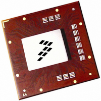
MPC8560CPX667JC Freescale Semiconductor, MPC8560CPX667JC Datasheet - Page 103

MPC8560CPX667JC
Manufacturer Part Number
MPC8560CPX667JC
Description
IC MPU PWRQUICC III 783-FCPBGA
Manufacturer
Freescale Semiconductor
Series
PowerQUICC IIIr
Specifications of MPC8560CPX667JC
Processor Type
MPC85xx PowerQUICC III 32-Bit
Speed
667MHz
Voltage
1.2V
Mounting Type
Surface Mount
Package / Case
783-FCPBGA
Core Size
32 Bit
Program Memory Size
64KB
Cpu Speed
667MHz
Embedded Interface Type
I2C, MII, SPI, TDM, UTOPIA
Digital Ic Case Style
BGA
No. Of Pins
783
Rohs Compliant
No
Family Name
MPC85XX
Device Core
PowerQUICC III
Device Core Size
32b
Frequency (max)
667MHz
Instruction Set Architecture
RISC
Supply Voltage 1 (typ)
1.2V
Operating Supply Voltage (max)
1.26V
Operating Supply Voltage (min)
1.14V
Operating Temp Range
-40C to 105C
Operating Temperature Classification
Industrial
Mounting
Surface Mount
Pin Count
783
Package Type
FCBGA
For Use With
MPC8560ADS-BGA - BOARD APPLICATION DEV 8560
Lead Free Status / RoHS Status
Contains lead / RoHS non-compliant
Features
-
Lead Free Status / Rohs Status
Not Compliant
Available stocks
Company
Part Number
Manufacturer
Quantity
Price
Company:
Part Number:
MPC8560CPX667JC
Manufacturer:
Freescale Semiconductor
Quantity:
10 000
Freescale Semiconductor
Rev. No.
1.2
1.1
1
Section 1.1.1—Updated feature list.
Section 1.2.1.1—Updated notes for Table 1.
Section 1.2.1.2—Removed 5-V PCI interface overshoot and undershoot figure.
Section 1.2.1.3—Added this section to summarize impedance driver settings for various interfaces.
Section 1.4—Updated rows in Reset Initialization timing specifications table. Added a table with DLL and
PLL timing specifications.
Section 1.5.2.2—Updated note 6 of DDR SDRAM Output AC Timing Specifications table.
Section 1.7—Changed the minimum input low current from -600 to -15 μA for the RGMII DC electrical
characteristics.
Section 1.7.2—Changed LCS[3:4] to TSEC1_TXD[6:5]. Updated notes regarding LCS[3:4].
Section 1.13.2—Updated the mechanical dimensions diagram for the package.
Section 1.13.3—Updated the notes for LBCTL, TRIG_OUT, and ASLEEP. Corrected pin assignments
for IIC_SDA and IIC_SCL. Corrected reserved pin assignment of V11 to U11. V11 is actually PCI_STOP.
Section 1.14.1—Updated the table for frequency options with respect to platform/CCB frequencies.
Section 1.14.4—Edited Frequency options with respect to memory bus speeds.
Made updates throughout document.
Section 1.6.1—Added symbols and note for the GTX_CLK125 timing parameters.
Section 1.11.3—Updated pin list table: LGPL5/LSDAMUX to LGPL5, LA[27:29] and LA[30:31] to
LA[27:31], TRST to TRST, added GBE Clocking section and EC_GTX_CLK125 signal.
Figure 50—Updated pin 2 connection information.
Original Customer Version.
MPC8560 Integrated Processor Hardware Specifications, Rev. 4.2
Table 62. Document Revision History (continued)
Substantive Change(s)
Document Revision History
103


