MPC8347CVRAGDB Freescale Semiconductor, MPC8347CVRAGDB Datasheet - Page 17
MPC8347CVRAGDB
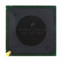
Manufacturer Part Number
MPC8347CVRAGDB
Description
IC MPU POWERQUICC II 620-PBGA
Manufacturer
Freescale Semiconductor
Series
PowerQUICC II PROr
Specifications of MPC8347CVRAGDB
Processor Type
MPC83xx PowerQUICC II Pro 32-Bit
Speed
400MHz
Voltage
1.2V
Mounting Type
Surface Mount
Package / Case
620-PBGA
Core Size
32 Bit
Program Memory Size
64KB
Cpu Speed
400MHz
Embedded Interface Type
I2C, SPI, USB, UART
Digital Ic Case Style
BGA
No. Of Pins
672
Rohs Compliant
Yes
Lead Free Status / RoHS Status
Lead free / RoHS Compliant
Features
-
Available stocks
Company
Part Number
Manufacturer
Quantity
Price
Company:

Part Number:
MPC8347CVRAGDB
Manufacturer:
FREESCA
Quantity:
13
Company:
Part Number:
MPC8347CVRAGDB
Manufacturer:
Freescale Semiconductor
Quantity:
10 000


Table 15
Table 16
6.2
This section provides the AC electrical characteristics for the DDR and DDR2 SDRAM interface.
6.2.1
Table 17
Table 18
Freescale Semiconductor
At recommended operating conditions with GV
At recommended operating conditions with GV
Current draw for MV
Note:
1. The voltage regulator for MV
AC input low voltage
AC input high voltage
AC input low voltage
AC input high voltage
Input/output capacitance: DQ, DQS
Delta input/output capacitance: DQ, DQS
Note:
1. This parameter is sampled. GV
provides the DDR capacitance when
provides the current draw characteristics for MV
provides the input AC timing specifications for the DDR2 SDRAM when GV
provides the input AC timing specifications for the DDR SDRAM when GV
DDR and DDR2 SDRAM AC Electrical Characteristics
MPC8347EA PowerQUICC II Pro Integrated Host Processor Hardware Specifications, Rev. 11
DDR and DDR2 SDRAM Input AC Timing Specifications
Parameter
Parameter
Table 17. DDR2 SDRAM Input AC Timing Specifications for 1.8-V Interface
Parameter/Condition
Table 18. DDR SDRAM Input AC Timing Specifications for 2.5-V Interface
REF
Parameter/Condition
Table 15. DDR SDRAM Capacitance for GV
REF
Table 16. Current Draw Characteristics for MV
DD
must supply up to 500 μA current.
= 2.5 V ± 0.125 V, f = 1 MHz, T
DD
DD
of 1.8 ± 5%.
of 2.5 ± 5%.
Symbol
Symbol
V
V
V
V
IH
IH
IL
IL
GV
DD
(typ) = 2.5 V.
Symbol
MV
MV
C
C
DIO
IO
Symbol
I
REF
REF
A
MVREF
REF
Min
Min
= 25°C, V
—
—
+ 0.25
+ 0.31
.
DD
OUT
Min
—
6
(typ) = 2.5 V
Min
—
= GV
MV
MV
REF
DD
REF
REF
Max
Max
/2, V
—
—
– 0.25
– 0.31
Max
0.5
Max
500
8
OUT
(peak-to-peak) = 0.2 V.
DD
DDR and DDR2 SDRAM
DD
(typ) = 2.5 V.
Unit
Unit
Unit
Unit
(typ) = 1.8 V.
pF
pF
μA
V
V
V
V
Notes
Notes
Notes
Note
—
—
—
—
1
1
1
17
Related parts for MPC8347CVRAGDB
Image
Part Number
Description
Manufacturer
Datasheet
Request
R

Part Number:
Description:
Manufacturer:
Freescale Semiconductor, Inc
Datasheet:
Part Number:
Description:
Manufacturer:
Freescale Semiconductor, Inc
Datasheet:
Part Number:
Description:
Manufacturer:
Freescale Semiconductor, Inc
Datasheet:
Part Number:
Description:
Manufacturer:
Freescale Semiconductor, Inc
Datasheet:
Part Number:
Description:
Manufacturer:
Freescale Semiconductor, Inc
Datasheet:
Part Number:
Description:
Manufacturer:
Freescale Semiconductor, Inc
Datasheet:
Part Number:
Description:
Manufacturer:
Freescale Semiconductor, Inc
Datasheet:
Part Number:
Description:
Manufacturer:
Freescale Semiconductor, Inc
Datasheet:
Part Number:
Description:
Manufacturer:
Freescale Semiconductor, Inc
Datasheet:
Part Number:
Description:
Manufacturer:
Freescale Semiconductor, Inc
Datasheet:
Part Number:
Description:
Manufacturer:
Freescale Semiconductor, Inc
Datasheet:
Part Number:
Description:
Manufacturer:
Freescale Semiconductor, Inc
Datasheet:
Part Number:
Description:
Manufacturer:
Freescale Semiconductor, Inc
Datasheet:
Part Number:
Description:
Manufacturer:
Freescale Semiconductor, Inc
Datasheet:
Part Number:
Description:
Manufacturer:
Freescale Semiconductor, Inc
Datasheet: