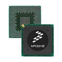
MPC8313CVRADDB Freescale Semiconductor, MPC8313CVRADDB Datasheet - Page 17

MPC8313CVRADDB
Manufacturer Part Number
MPC8313CVRADDB
Description
MPU POWERQUICC II PRO 516-PBGA
Manufacturer
Freescale Semiconductor
Datasheet
1.MPC8313CZQAFFB.pdf
(100 pages)
Specifications of MPC8313CVRADDB
Processor Type
MPC83xx PowerQUICC II Pro 32-Bit
Speed
267MHz
Voltage
0.95 V ~ 1.05 V
Mounting Type
Surface Mount
Package / Case
516-PBGA
Processor Series
MPC8xxx
Core
e300
Data Bus Width
32 bit
Development Tools By Supplier
MPC8313E-RDB
Maximum Clock Frequency
400 MHz
Operating Supply Voltage
- 0.3 V to + 1.26 V
Maximum Operating Temperature
+ 105 C
Mounting Style
SMD/SMT
Data Ram Size
16 KB
I/o Voltage
2.5 V
Interface Type
I2C, SPI, UART
Minimum Operating Temperature
- 40 C
Program Memory Type
EEPROM/Flash
Lead Free Status / RoHS Status
Lead free / RoHS Compliant
Features
-
Lead Free Status / Rohs Status
Lead free / RoHS Compliant
Available stocks
Company
Part Number
Manufacturer
Quantity
Price
Company:
Part Number:
MPC8313CVRADDB
Manufacturer:
FREESCAL
Quantity:
672
Company:
Part Number:
MPC8313CVRADDB
Manufacturer:
Freescale Semiconductor
Quantity:
10 000
Figure 4
6.2.2
Freescale Semiconductor
MCK[ n ] cycle time, MCK[ n ]/MCK[ n ] crossing
ADDR/CMD output setup with respect to MCK
ADDR/CMD output hold with respect to MCK
MCS[ n ] output setup with respect to MCK
MCS[ n ] output hold with respect to MCK
MCK to MDQS Skew
MDQ//MDM output setup with respect to
MDQS
MDQ//MDM output hold with respect to MDQS
MDQS preamble start
illustrates the DDR input timing diagram showing the t
Table 20. DDR and DDR2 SDRAM Output AC Timing Specifications for Rev. 1.0 Silicon
MDQS[ n ]
DDR and DDR2 SDRAM Output AC Timing Specifications
MDQ[ x ]
MCK[ n ]
MCK[ n ]
Parameter
MPC8313E PowerQUICC
333 MHz
266 MHz
333 MHz
266 MHz
333 MHz
266 MHz
333 MHz
266 MHz
333 MHz
266 MHz
333 MHz
266 MHz
t
t
MCK
Figure 4. DDR Input Timing Diagram
DISKEW
™
Symbol
t
t
t
t
t
t
t
t
t
t
DDKHMH
DDKHDS,
DDKHDX,
DDKHMP
DDKHAS
DDKHAX
DDKHCS
DDKHCX
DDKLDS
DDKLDX
II Pro Processor Hardware Specifications, Rev. 3
t
MCK
D0
1
–0.5 × t
D1
t
DISKEW
3.15
–0.6
1100
Min
3.15
3.15
800
900
900
2.1
2.5
2.4
2.4
2.4
MCK
6
– 0.6
DISKEW
–0.5 × t
timing parameter.
Max
0.6
10
—
—
—
—
—
—
—
—
—
—
—
—
MCK
+ 0.6
DDR and DDR2 SDRAM
Unit
ns
ns
ns
ns
ns
ns
ps
ps
ns
Notes
2
4
6
3
3
3
3
5
5
17


