MPC8379EVRAJF Freescale Semiconductor, MPC8379EVRAJF Datasheet - Page 46
MPC8379EVRAJF
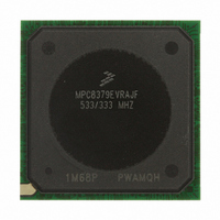
Manufacturer Part Number
MPC8379EVRAJF
Description
MPU PWRQUICC II 533MHZ 689TEPBGA
Manufacturer
Freescale Semiconductor
Series
PowerQUICC II PROr
Datasheets
1.MPC8377EVRAGD.pdf
(126 pages)
2.MPC8377EVRAGD.pdf
(2 pages)
3.MPC8379VRAGD.pdf
(116 pages)
Specifications of MPC8379EVRAJF
Processor Type
MPC83xx PowerQUICC II Pro 32-Bit
Speed
533MHz
Voltage
1V
Mounting Type
Surface Mount
Package / Case
689-TePBGA II
Maximum Clock Frequency
533 MHz
Operating Supply Voltage
1.8 V to 2.5 V
Maximum Operating Temperature
+ 105 C
Mounting Style
SMD/SMT
I/o Voltage
1.8 V, 2.5 V, 3.3 V
Minimum Operating Temperature
0 C
Core Size
32 Bit
Program Memory Size
64KB
Cpu Speed
533MHz
Embedded Interface Type
DUART, HSSI, I2C, IPIC, JTAG, SPI, USB
Digital Ic Case Style
BGA
No. Of Pins
689
Rohs Compliant
Yes
For Use With
MPC8377E-RDBA - BOARD REF DES MPC8377 REV 2.1MPC8377E-MDS-PB - BOARD MODULAR DEV SYSTEM
Lead Free Status / RoHS Status
Lead free / RoHS Compliant
Features
-
Lead Free Status / Rohs Status
Lead free / RoHS Compliant
Available stocks
Company
Part Number
Manufacturer
Quantity
Price
Company:

Part Number:
MPC8379EVRAJF
Manufacturer:
Freescale Semiconductor
Quantity:
135
Company:
Part Number:
MPC8379EVRAJF
Manufacturer:
Freescale Semiconductor
Quantity:
10 000


Enhanced Secure Digital Host Controller (eSDHC)
11.2.1
Figure 27
11.2.1.1
The following equations show how to calculate the allowed skew range between the SD_CLK and
SD_DAT/CMD signals on the PCB.
No clock delay:
With clock delay:
This means that data can be delayed versus clock up to 11 ns in ideal case of t
11.2.1.2
The following equations show how to calculate the allowed skew range between the SD_CLK and
SD_DAT/CMD signals on the PCB.
46
t
t
DATA_DELAY
DATA_DELAY
provides the data and command output timing diagram.
Full-Speed Output Path (Write)
Full-Speed Write Meeting Setup (Maximum Delay)
Full-Speed Write Meeting Hold (Minimum Delay)
MPC8377E Pins
MPC8377E Pins
MPC8377E Pin
Output from the
SD CLK at the
the Card Pin
Input at the
MPC8377E PowerQUICC II Pro Processor Hardware Specifications, Rev. 4
t
SD CLK at
DATA_DELAY
+ 20 < 40 + t
< 11 + t
t
SFSKHOV
t
CLK_DELAY
Output Valid Time: t
Output Hold Time: t
CLK_DELAY
t
SFSKHOV
+ t
+ t
SFSCKL
CLK_DELAY
DATA_DELAY
< t
Figure 27. Full Speed Output Path
SFSCKL
+ t
< t
DATA_DELAY
t
SFSCK
SFSKHOV
SFSKHOX
SFSCK
Driving
+ t
Edge
t
DATA_DELAY
–
+ t
SFSKHOX
5
(Clock Cycle)
ISU
–
+ t
4
< t
CLK_DELAY
+ t
SFSCKL
ISU
+ t
DATA_DELAY
< t
t
t
SFSCKL
CLK_DELAY
ISU
+ t
–
t
t
CLK_DELAY
(5 ns)
ISU
SFSCKL
–
t
–
SFSKHOV
t
IH
Sampling
Edge
SFSCKL
t
IH
(5 ns)
Freescale Semiconductor
= 20 ns:
Eqn. 1
Eqn. 2
Eqn. 3
Eqn. 4
Related parts for MPC8379EVRAJF
Image
Part Number
Description
Manufacturer
Datasheet
Request
R

Part Number:
Description:
BOARD REF DESIGN MPC8379E
Manufacturer:
Freescale Semiconductor
Datasheet:

Part Number:
Description:
BOARD REFERENCE FOR MPC837
Manufacturer:
Freescale Semiconductor
Datasheet:
Part Number:
Description:
BOARD PROCESSOR FOR MDS S
Manufacturer:
Freescale Semiconductor
Datasheet:

Part Number:
Description:
Powerquicc Ii Pro Processor Hardware Specifications
Manufacturer:
Freescale Semiconductor, Inc
Datasheet:

Part Number:
Description:
BOARD REF DES MPC8377 REV 2.1
Manufacturer:
Freescale Semiconductor
Datasheet:
Part Number:
Description:
Manufacturer:
Freescale Semiconductor, Inc
Datasheet:
Part Number:
Description:
Manufacturer:
Freescale Semiconductor, Inc
Datasheet:
Part Number:
Description:
Manufacturer:
Freescale Semiconductor, Inc
Datasheet:
Part Number:
Description:
Manufacturer:
Freescale Semiconductor, Inc
Datasheet:
Part Number:
Description:
Manufacturer:
Freescale Semiconductor, Inc
Datasheet:
Part Number:
Description:
Manufacturer:
Freescale Semiconductor, Inc
Datasheet:
Part Number:
Description:
Manufacturer:
Freescale Semiconductor, Inc
Datasheet:
Part Number:
Description:
Manufacturer:
Freescale Semiconductor, Inc
Datasheet:
Part Number:
Description:
Manufacturer:
Freescale Semiconductor, Inc
Datasheet:
Part Number:
Description:
Manufacturer:
Freescale Semiconductor, Inc
Datasheet: