MPC8347VRADDB Freescale Semiconductor, MPC8347VRADDB Datasheet - Page 95
MPC8347VRADDB
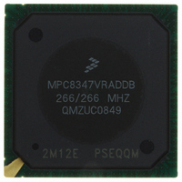
Manufacturer Part Number
MPC8347VRADDB
Description
IC MPU POWERQUICC II 620-PBGA
Manufacturer
Freescale Semiconductor
Series
PowerQUICC II PROr
Specifications of MPC8347VRADDB
Processor Type
MPC83xx PowerQUICC II Pro 32-Bit
Speed
266MHz
Voltage
1.2V
Mounting Type
Surface Mount
Package / Case
620-PBGA
Processor Series
MPC8xxx
Core
e300
Data Bus Width
32 bit
Development Tools By Supplier
MPC8349E-MITXE
Maximum Clock Frequency
266 MHz
Maximum Operating Temperature
+ 105 C
Mounting Style
SMD/SMT
I/o Voltage
1.8 V, 2.5 V, 3.3 V
Minimum Operating Temperature
0 C
Core Size
32 Bit
Program Memory Size
64KB
Cpu Speed
266MHz
Embedded Interface Type
I2C, SPI, USB, UART
Digital Ic Case Style
BGA
No. Of Pins
672
Rohs Compliant
Yes
Lead Free Status / RoHS Status
Lead free / RoHS Compliant
Features
-
Lead Free Status / Rohs Status
Lead free / RoHS Compliant
Available stocks
Company
Part Number
Manufacturer
Quantity
Price
Company:

Part Number:
MPC8347VRADDB
Manufacturer:
Freescale Semiconductor
Quantity:
135
Company:
Part Number:
MPC8347VRADDB
Manufacturer:
Freescale Semiconductor
Quantity:
10 000


22 Document Revision History
Table 66
Freescale Semiconductor
Revision
11
10
9
provides a revision history of this document.
MPC8347E PowerQUICC™ II Pro Integrated Host Processor Hardware Specifications, Rev. 11
2/2009
4/2007
3/2007
Date
In
In
independent filter circuits,” and “the five AVDD pins” to provide four independent filter circuits,” and
“the four AVDD pins.”
In
that the device does not follow the I2C-BUS Specifications version 2.1 regarding the t
parameter.
In
In
In
DLL bypass mode). Similarly, made the same correction to
output signals.
Added
In
Added footnote 4 to
In
is up to 667(TBGA) with a platform frequency of 333 and limited to 400 (PBGA) with a platform
frequency of 266.”
Added footnote 10 and 11 to
In
Added footnote 6 to
In
In 8.1.1, removed the note “The potential applied to the input of a GMII, MII, TBI, RGMII, or RTBI
receiver may exceed the potential of the receiver power supply (that is, a RGMII driver powered from
a 3.6 V supply driving VOH into a RGMII receiver powered from a 2.5-V supply). Tolerance for
dissimilar RGMII driver and receiver supply potentials is implicit in these specifications.”
In
added USB to the seventh row.
In
In
paragraph, added a new paragraph.
Deleted Section 21.8, “JTAG Configuration Signals,” and Figure 43, “JTAG Interface Connection.”
In Table 54, “Operating Frequencies for TBGA,” in the ‘Coherent system bus frequency ( csb_clk )’
row, changed the value in the 533 MHz column to 100–333.
In Table 60, “Suggested PLL Configurations,” under the subhead, ‘33 MHz CLKIN/PCI_CLK
Options,’ added row A03 between Ref. No. 724 and 804. Under the subhead ‘66 MHz
CLKIN/PCI_CLK Options,’ added row 503 between Ref. No. 305 and 404. For Ref. No. 306, changed
the CORE PLL value to 0000110.
In Section 23, “Ordering Information,” replaced first paragraph and added a note.
In Section 23.1, “Part Numbers Fully Addressed by This Document,” replaced first paragraph.
Table
Table
Section 21.1, “System
Section 21.2, “PLL Power Supply
Table
Table
Table
Table
Table
Table
Table
Table
Section 21.7, “Pull-Up Resistor Requirements,”
pull-up resistor. For proper functionality of the device, this pin must be pulled up or actively driven
high during a hard reset. No external pull-down resistors are allowed to be attached to this net.”
1% input frequency down-spread at maximum 50KHz modulation rate regardless of input
frequency.”
Figure 1
35, removed row for rise time (t
35, corrected t
54, corrected the max csb_clk to 266 MHz.
60, added PLL configurations 903, 923, A03, A23, and 503 for 533 MHz
9.2, clarified that AC table is for ULPI only.
67, updated note 1 to say the following: “For temperature range = C, processor frequency
51,
7, updated the note 6 to say the following: “The Spread spectrum clocking. Is allowed with
3,
54,
“Output Drive Capability,”
Table
“Operating Frequencies for TBGA,”
Table 66. Document Revision History
and
52, updated note 11 to say the following: “SEC1_TXD[3] is required an external
Table
Table
Figure
LBKHOV
Clocking,” removed “(AVDD1)” and “(AVDD2”) from bulleted list.
67.
7.
4.
Table 51
parametr to t
Filtering,” in the second paragraph, changed “provide five
changed the values in the Output Impedance column and
Substantive Change(s)
and
I2CR
). Removed minimum value of t
Table
LBKLOV
added column for 400 MHz.
52.
deleted last two paragraphs and after first
(output data is driven on falling edge of clock in
Figure
21,
Figure
Document Revision History
I2CF
. Added note 5 stating
23, and
Figure 24
I2CF
AC
for
95
Related parts for MPC8347VRADDB
Image
Part Number
Description
Manufacturer
Datasheet
Request
R

Part Number:
Description:
Integrated Host Processor Hardware Specifications
Manufacturer:
FREESCALE [Freescale Semiconductor, Inc]
Datasheet:

Part Number:
Description:
Manufacturer:
Freescale Semiconductor, Inc
Datasheet:
Part Number:
Description:
Manufacturer:
Freescale Semiconductor, Inc
Datasheet:
Part Number:
Description:
Manufacturer:
Freescale Semiconductor, Inc
Datasheet:
Part Number:
Description:
Manufacturer:
Freescale Semiconductor, Inc
Datasheet:
Part Number:
Description:
Manufacturer:
Freescale Semiconductor, Inc
Datasheet:
Part Number:
Description:
Manufacturer:
Freescale Semiconductor, Inc
Datasheet:
Part Number:
Description:
Manufacturer:
Freescale Semiconductor, Inc
Datasheet:
Part Number:
Description:
Manufacturer:
Freescale Semiconductor, Inc
Datasheet:
Part Number:
Description:
Manufacturer:
Freescale Semiconductor, Inc
Datasheet:
Part Number:
Description:
Manufacturer:
Freescale Semiconductor, Inc
Datasheet:
Part Number:
Description:
Manufacturer:
Freescale Semiconductor, Inc
Datasheet:
Part Number:
Description:
Manufacturer:
Freescale Semiconductor, Inc
Datasheet:
Part Number:
Description:
Manufacturer:
Freescale Semiconductor, Inc
Datasheet:
Part Number:
Description:
Manufacturer:
Freescale Semiconductor, Inc
Datasheet: