MPC8347VRADDB Freescale Semiconductor, MPC8347VRADDB Datasheet - Page 15
MPC8347VRADDB
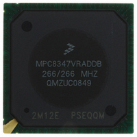
Manufacturer Part Number
MPC8347VRADDB
Description
IC MPU POWERQUICC II 620-PBGA
Manufacturer
Freescale Semiconductor
Series
PowerQUICC II PROr
Specifications of MPC8347VRADDB
Processor Type
MPC83xx PowerQUICC II Pro 32-Bit
Speed
266MHz
Voltage
1.2V
Mounting Type
Surface Mount
Package / Case
620-PBGA
Processor Series
MPC8xxx
Core
e300
Data Bus Width
32 bit
Development Tools By Supplier
MPC8349E-MITXE
Maximum Clock Frequency
266 MHz
Maximum Operating Temperature
+ 105 C
Mounting Style
SMD/SMT
I/o Voltage
1.8 V, 2.5 V, 3.3 V
Minimum Operating Temperature
0 C
Core Size
32 Bit
Program Memory Size
64KB
Cpu Speed
266MHz
Embedded Interface Type
I2C, SPI, USB, UART
Digital Ic Case Style
BGA
No. Of Pins
672
Rohs Compliant
Yes
Lead Free Status / RoHS Status
Lead free / RoHS Compliant
Features
-
Lead Free Status / Rohs Status
Lead free / RoHS Compliant
Available stocks
Company
Part Number
Manufacturer
Quantity
Price
Company:

Part Number:
MPC8347VRADDB
Manufacturer:
Freescale Semiconductor
Quantity:
135
Company:
Part Number:
MPC8347VRADDB
Manufacturer:
Freescale Semiconductor
Quantity:
10 000


6
This section describes the DC and AC electrical specifications for the DDR SDRAM interface of the
MPC8347E.
6.1
Table 11
MPC8347E.
Table 12
Freescale Semiconductor
I/O supply voltage
I/O reference voltage
I/O termination voltage
Input high voltage
Input low voltage
Output leakage current
Output high current (V
Output low current (V
MV
Notes:
1. GV
2. MV
3. V
4. Output leakage is measured with all outputs disabled, 0 V
Input/output capacitance: DQ, DQS
Delta input/output capacitance: DQ, DQS
Note:
1. This parameter is sampled. GV
noise on MV
equal to MV
REF
TT
DD
REF
is not applied directly to the device. It is the supply to which far end signal termination is made and is expected to be
input leakage current
DDR SDRAM
is expected to be within 50 mV of the DRAM GV
is expected to be equal to 0.5 × GV
provides the recommended operating conditions for the DDR SDRAM component(s) of the
provides the DDR capacitance.
DDR SDRAM DC Electrical Characteristics
MPC8347E PowerQUICC™ II Pro Integrated Host Processor Hardware Specifications, Rev. 11
Parameter/Condition
REF
REF
The information in this document is accurate for revision 1.1 silicon and
earlier. For information on revision 3.0 silicon and earlier versions see the
MPC8347EA PowerQUICC™ II Pro Integrated Host Processor Hardware
Specifications. See
Document,” for silicon revision level determination.
. This rail should track variations in the DC level of MV
Parameter/Condition
may not exceed ±2% of the DC value.
OUT
OUT
= 0.35 V)
= 1.95 V)
Table 11. DDR SDRAM DC Electrical Characteristics
DD
= 2.5 V ± 0.125 V, f = 1 MHz, T
Section 23.1, “Part Numbers Fully Addressed by This
Table 12. DDR SDRAM Capacitance
DD
, and to track GV
Symbol
MV
GV
I
VREF
V
V
I
V
I
I
OH
OZ
OL
TT
REF
IH
IL
DD
DD
NOTE
at all times.
≤
V
Symbol
OUT
DD
C
C
DIO
MV
MV
A
IO
0.49 × GV
DC variations as measured at the receiver. Peak-to-peak
≤
= 25°C, V
GV
REF
REF
2.375
–15.2
REF
–0.3
15.2
Min
–10
—
DD
– 0.04
+ 0.18
.
.
DD
OUT
Min
—
6
= GV
MV
MV
0.51 × GV
GV
DD
REF
REF
2.625
/2, V
DD
Max
10
—
—
5
+ 0.04
– 0.18
Max
+ 0.3
0.5
OUT
8
DD
(peak-to-peak) = 0.2 V.
Unit
Unit
mA
mA
μA
μA
pF
pF
V
V
V
V
V
DDR SDRAM
Notes
Notes
1
2
1
3
4
1
15
Related parts for MPC8347VRADDB
Image
Part Number
Description
Manufacturer
Datasheet
Request
R

Part Number:
Description:
Integrated Host Processor Hardware Specifications
Manufacturer:
FREESCALE [Freescale Semiconductor, Inc]
Datasheet:

Part Number:
Description:
Manufacturer:
Freescale Semiconductor, Inc
Datasheet:
Part Number:
Description:
Manufacturer:
Freescale Semiconductor, Inc
Datasheet:
Part Number:
Description:
Manufacturer:
Freescale Semiconductor, Inc
Datasheet:
Part Number:
Description:
Manufacturer:
Freescale Semiconductor, Inc
Datasheet:
Part Number:
Description:
Manufacturer:
Freescale Semiconductor, Inc
Datasheet:
Part Number:
Description:
Manufacturer:
Freescale Semiconductor, Inc
Datasheet:
Part Number:
Description:
Manufacturer:
Freescale Semiconductor, Inc
Datasheet:
Part Number:
Description:
Manufacturer:
Freescale Semiconductor, Inc
Datasheet:
Part Number:
Description:
Manufacturer:
Freescale Semiconductor, Inc
Datasheet:
Part Number:
Description:
Manufacturer:
Freescale Semiconductor, Inc
Datasheet:
Part Number:
Description:
Manufacturer:
Freescale Semiconductor, Inc
Datasheet:
Part Number:
Description:
Manufacturer:
Freescale Semiconductor, Inc
Datasheet:
Part Number:
Description:
Manufacturer:
Freescale Semiconductor, Inc
Datasheet:
Part Number:
Description:
Manufacturer:
Freescale Semiconductor, Inc
Datasheet: