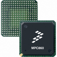
MPC857DSLVR50B Freescale Semiconductor, MPC857DSLVR50B Datasheet - Page 3

MPC857DSLVR50B
Manufacturer Part Number
MPC857DSLVR50B
Description
IC MPU POWERQUICC 50MHZ 357-PBGA
Manufacturer
Freescale Semiconductor
Datasheet
1.MPC857TVR100B.pdf
(88 pages)
Specifications of MPC857DSLVR50B
Processor Type
MPC8xx PowerQUICC 32-Bit
Speed
50MHz
Voltage
3.3V
Mounting Type
Surface Mount
Package / Case
357-PBGA
Processor Series
MPC85xx
Core
MPC8xx
Data Bus Width
32 bit
Maximum Clock Frequency
50 MHz
Operating Supply Voltage
2.5 V, 3.3 V
Maximum Operating Temperature
+ 105 C
Mounting Style
SMD/SMT
Minimum Operating Temperature
0 C
Family Name
MPC8xx
Device Core
PowerQUICC
Device Core Size
32b
Frequency (max)
50MHz
Instruction Set Architecture
RISC
Supply Voltage 1 (typ)
2.5/3.3V
Operating Supply Voltage (max)
3.465/3.6V
Operating Supply Voltage (min)
2/3.135V
Operating Temp Range
0C to 105C
Operating Temperature Classification
Commercial
Mounting
Surface Mount
Pin Count
357
Package Type
BGA
Leaded Process Compatible
Yes
Rohs Compliant
Yes
Peak Reflow Compatible (260 C)
Yes
Lead Free Status / RoHS Status
Lead free / RoHS Compliant
Features
-
Lead Free Status / Rohs Status
Lead free / RoHS Compliant
Available stocks
Company
Part Number
Manufacturer
Quantity
Price
Company:
Part Number:
MPC857DSLVR50B
Manufacturer:
Freescale Semiconductor
Quantity:
135
Company:
Part Number:
MPC857DSLVR50B
Manufacturer:
Freescale Semiconductor
Quantity:
10 000
Freescale Semiconductor
•
•
•
•
•
•
The MPC862/857T/857DSL provides enhanced ATM functionality over that of the MPC860SAR.
The MPC862/857T/857DSL adds major new features available in “enhanced SAR” (ESAR) mode,
including the following:
— Improved operation, administration and maintenance (OAM) support
— OAM performance monitoring (PM) support
— Multiple APC priority levels available to support a range of traffic pace requirements
— ATM port-to-port switching capability without the need for RAM-based microcode
— Simultaneous MII (10/100Base-T) and UTOPIA (half-duplex) capability
— Optional statistical cell counters per PHY
— UTOPIA level 2 compliant interface with added FIFO buffering to reduce the total cell
— Multi-PHY support on the MPC857T
— Four PHY support on the MPC857DSL
— Parameter RAM for both SPI and I
— Supports full-duplex UTOPIA both master (ATM side) and slave (PHY side) operation using
— AAL2/VBR functionality is ROM-resident
Up to 32-bit data bus (dynamic bus sizing for 8, 16, and 32 bits)
32 address lines
Memory controller (eight banks)
— Contains complete dynamic RAM (DRAM) controller
— Each bank can be a chip select or RAS to support a DRAM bank
— Up to 30 wait states programmable per memory bank
— Glueless interface to Page mode/EDO/SDRAM, SRAM, EPROMs, flash EPROMs, and other
— DRAM controller programmable to support most size and speed memory interfaces
— Four CAS lines, four WE lines, one OE line
— Boot chip-select available at reset (options for 8-, 16-, or 32-bit memory)
— Variable block sizes (32 Kbyte–256 Mbyte)
— Selectable write protection
— On-chip bus arbitration logic
General-purpose timers
— Four 16-bit timers cascadable to be two 32-bit timers
— Gate mode can enable/disable counting
— Interrupt can be masked on reference match and event capture
Fast Ethernet controller (FEC)
— Simultaneous MII (10/100Base-T) and UTOPIA operation when using the UTOPIA
transmission time. (The earlier UTOPIA level 1 specification is also supported.)
a “split” bus
memory devices.
multiplexed bus.
MPC862/857T/857DSL PowerQUICC™ Family Hardware Specifications, Rev. 3
2
C can be relocated without RAM-based microcode
Features
3


