MPC8541EVTAPF Freescale Semiconductor, MPC8541EVTAPF Datasheet - Page 49
MPC8541EVTAPF
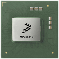
Manufacturer Part Number
MPC8541EVTAPF
Description
IC MPU POWERQUICC III 783-FCPBGA
Manufacturer
Freescale Semiconductor
Series
PowerQUICC IIIr
Specifications of MPC8541EVTAPF
Processor Type
MPC85xx PowerQUICC III 32-Bit
Speed
833MHz
Voltage
1.2V
Mounting Type
Surface Mount
Package / Case
783-FCPBGA
Core Size
32 Bit
Program Memory Size
64KB
Cpu Speed
833MHz
Digital Ic Case Style
BGA
No. Of Pins
783
Supply Voltage Range
1.14V To 1.26V
Rohs Compliant
Yes
Family Name
MPC85XX
Device Core
PowerQUICC III
Device Core Size
32b
Frequency (max)
833MHz
Instruction Set Architecture
RISC
Supply Voltage 1 (typ)
1.2V
Operating Supply Voltage (max)
1.26V
Operating Supply Voltage (min)
1.14V
Operating Temp Range
0C to 105C
Operating Temperature Classification
Commercial
Mounting
Surface Mount
Pin Count
783
Package Type
FCBGA
For Use With
MPC8548CDS - DEV TOOLS CDS FOR 8548CWH-PPC-8540N-VE - KIT EVAL SYSTEM MPC8540
Lead Free Status / RoHS Status
Lead free / RoHS Compliant
Features
-
Lead Free Status / Rohs Status
Compliant
Available stocks
Company
Part Number
Manufacturer
Quantity
Price
Company:

Part Number:
MPC8541EVTAPF
Manufacturer:
FREE
Quantity:
12
Company:
Part Number:
MPC8541EVTAPF
Manufacturer:
Freescale Semiconductor
Quantity:
10 000
Part Number:
MPC8541EVTAPF
Manufacturer:
FREESCALE
Quantity:
20 000
Company:
Part Number:
MPC8541EVTAPFF
Manufacturer:
FREESCAL
Quantity:
210


Figure 31
Figure 32
Figure 33
Figure 34
Freescale Semiconductor
MPC8541E PowerQUICC™ III Integrated Communications Processor Hardware Specification, Rev. 4.2
provides the AC test load for TDO and the boundary-scan outputs of the MPC8541E.
provides the JTAG clock input timing diagram.
provides the TRST timing diagram.
provides the boundary-scan timing diagram.
External Clock
Data Outputs
Data Outputs
Data Inputs
External Clock
Boundary
Boundary
Boundary
TRST
JTAG
JTAG
Output
t
Output Data Valid
JTKLDX
Figure 31. AC Test Load for the JTAG Interface
Figure 32. JTAG Clock Input Timing Diagram
Figure 34. Boundary-Scan Timing Diagram
VM
t
JTKHKL
Figure 33. TRST Timing Diagram
VM
t
Z
VM
JTKLDZ
VM = Midpoint Voltage (OV DD /2)
VM = Midpoint Voltage (OV DD /2)
VM = Midpoint Voltage (OV DD /2)
t
0
JTKLDV
t
= 50 Ω
JTG
VM
t
TRST
t
JTDVKH
VM
R
VM
Output Data Valid
L
Data Valid
= 50 Ω
Input
t
JTGR
VM
OV
DD
t
t
JTDXKH
JTGF
/2
JTAG
49
Related parts for MPC8541EVTAPF
Image
Part Number
Description
Manufacturer
Datasheet
Request
R

Part Number:
Description:
Manufacturer:
Freescale Semiconductor, Inc
Datasheet:
Part Number:
Description:
Manufacturer:
Freescale Semiconductor, Inc
Datasheet:
Part Number:
Description:
Manufacturer:
Freescale Semiconductor, Inc
Datasheet:
Part Number:
Description:
Manufacturer:
Freescale Semiconductor, Inc
Datasheet:
Part Number:
Description:
Manufacturer:
Freescale Semiconductor, Inc
Datasheet:
Part Number:
Description:
Manufacturer:
Freescale Semiconductor, Inc
Datasheet:
Part Number:
Description:
Manufacturer:
Freescale Semiconductor, Inc
Datasheet:
Part Number:
Description:
Manufacturer:
Freescale Semiconductor, Inc
Datasheet:
Part Number:
Description:
Manufacturer:
Freescale Semiconductor, Inc
Datasheet:
Part Number:
Description:
Manufacturer:
Freescale Semiconductor, Inc
Datasheet:
Part Number:
Description:
Manufacturer:
Freescale Semiconductor, Inc
Datasheet:
Part Number:
Description:
Manufacturer:
Freescale Semiconductor, Inc
Datasheet:
Part Number:
Description:
Manufacturer:
Freescale Semiconductor, Inc
Datasheet:
Part Number:
Description:
Manufacturer:
Freescale Semiconductor, Inc
Datasheet:
Part Number:
Description:
Manufacturer:
Freescale Semiconductor, Inc
Datasheet: