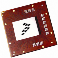
MPC8560PX833LB Freescale Semiconductor, MPC8560PX833LB Datasheet - Page 60

MPC8560PX833LB
Manufacturer Part Number
MPC8560PX833LB
Description
IC MPU POWERQUICC III 783-FCPBGA
Manufacturer
Freescale Semiconductor
Datasheet
1.MPC8560PX833LB.pdf
(104 pages)
Specifications of MPC8560PX833LB
Processor Type
MPC85xx PowerQUICC III 32-Bit
Speed
833MHz
Voltage
1.2V
Mounting Type
Surface Mount
Package / Case
783-FCPBGA
Family Name
MPC85XX
Device Core
PowerQUICC III
Device Core Size
32b
Frequency (max)
833MHz
Instruction Set Architecture
RISC
Supply Voltage 1 (typ)
1.2V
Operating Supply Voltage (max)
1.26V
Operating Supply Voltage (min)
1.14V
Operating Temp Range
0C to 105C
Operating Temperature Classification
Commercial
Mounting
Surface Mount
Pin Count
783
Package Type
FCBGA
For Use With
MPC8560ADS-BGA - BOARD APPLICATION DEV 8560
Lead Free Status / RoHS Status
Contains lead / RoHS non-compliant
Features
-
Lead Free Status / Rohs Status
Not Compliant
Available stocks
Company
Part Number
Manufacturer
Quantity
Price
Company:
Part Number:
MPC8560PX833LB
Manufacturer:
MOTOROLA
Quantity:
852
Company:
Part Number:
MPC8560PX833LB
Manufacturer:
Freescale Semiconductor
Quantity:
10 000
Part Number:
MPC8560PX833LB
Manufacturer:
NXP/恩智浦
Quantity:
20 000
RapidIO
To illustrate these definitions using numerical values, consider the case where a LVDS transmitter has a
common mode voltage of 1.2 V and each signal has a swing that goes between 1.4 and 1.0 V. Using these
values, the peak-to-peak voltage swing of the signals TD, TD, RD, and RD is 400 mV. The differential
signal ranges between 400 and –400 mV. The peak differential signal is 400 mV, and the peak-to-peak
differential signal is 800 mV.
A timing edge is the zero-crossing of a differential signal. Each skew timing parameter on a parallel bus
is synchronously measured on two signals relative to each other in the same cycle, such as data to data,
data to clock, or clock to clock. A skew timing parameter may be relative to the edge of a signal or to the
middle of two sequential edges.
Static skew represents the timing difference between signals that does not vary over time regardless of
system activity or data pattern. Path length differences are a primary source of static skew.
Dynamic skew represents the amount of timing difference between signals that is dependent on the activity
of other signals and varies over time. Crosstalk between signals is a source of dynamic skew.
Eye diagrams and compliance masks are a useful way to visualize and specify driver and receiver
performance. This technique is used in several serial bus specifications. An example compliance mask is
shown in
is source synchronous to its bus clock while serial data is referenced to its embedded clock. Eye diagrams
reveal the quality (cleanness, openness, goodness) of a driver output or receiver input. An advantage of
using an eye diagram and a compliance mask is that it allows specifying the quality of a signal without
requiring separate specifications for effects such as rise time, duty cycle distortion, data dependent
dynamic skew, random dynamic skew, etc. This allows the individual semiconductor manufacturer
maximum flexibility to trade off various performance criteria while keeping the system performance
constant.
In using the eye pattern and compliance mask approach, the quality of the signal is specified by the
compliance mask. The mask specifies the maximum permissible magnitude of the signal and the minimum
permissible eye opening. The eye diagram for the signal under test is generated according to the
specification. Compliance is determined by whether the compliance mask can be positioned over the eye
diagram such that the eye pattern falls entirely within the unshaded portion of the mask.
Serial specifications have clock encoded with the data, but the LP-LVDS physical layer defined by
RapidIO is a source synchronous parallel port so additional specifications to include effects that are not
found in serial links are required. Specifications for the effect of bit to bit timing differences caused by
static skew have been added and the eye diagrams specified are measured relative to the associated clock
in order to include clock to data effects. With the transmit output (or receiver input) eye diagram, the user
can determine if the transmitter output (or receiver input) is compliant with an oscilloscope with the
appropriate software.
60
•
•
The peak differential signal of the transmitter output or receiver input, is A – B volts.
The peak-to-peak differential signal of the transmitter output or receiver input, is 2 × (A – B) volts.
Figure
43. The key difference in the application of this technique for a parallel bus is that the data
Figure 42. Differential Peak-to-Peak Voltage of Transmitter or Receiver
MPC8560 Integrated Processor Hardware Specifications, Rev. 5
A V
B V
TD or RD
TD or RD
Freescale Semiconductor


