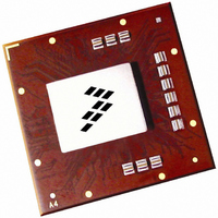
MPC8560PX833LB Freescale Semiconductor, MPC8560PX833LB Datasheet - Page 46

MPC8560PX833LB
Manufacturer Part Number
MPC8560PX833LB
Description
IC MPU POWERQUICC III 783-FCPBGA
Manufacturer
Freescale Semiconductor
Datasheet
1.MPC8560PX833LB.pdf
(104 pages)
Specifications of MPC8560PX833LB
Processor Type
MPC85xx PowerQUICC III 32-Bit
Speed
833MHz
Voltage
1.2V
Mounting Type
Surface Mount
Package / Case
783-FCPBGA
Family Name
MPC85XX
Device Core
PowerQUICC III
Device Core Size
32b
Frequency (max)
833MHz
Instruction Set Architecture
RISC
Supply Voltage 1 (typ)
1.2V
Operating Supply Voltage (max)
1.26V
Operating Supply Voltage (min)
1.14V
Operating Temp Range
0C to 105C
Operating Temperature Classification
Commercial
Mounting
Surface Mount
Pin Count
783
Package Type
FCBGA
For Use With
MPC8560ADS-BGA - BOARD APPLICATION DEV 8560
Lead Free Status / RoHS Status
Contains lead / RoHS non-compliant
Features
-
Lead Free Status / Rohs Status
Not Compliant
Available stocks
Company
Part Number
Manufacturer
Quantity
Price
Company:
Part Number:
MPC8560PX833LB
Manufacturer:
MOTOROLA
Quantity:
852
Company:
Part Number:
MPC8560PX833LB
Manufacturer:
Freescale Semiconductor
Quantity:
10 000
Part Number:
MPC8560PX833LB
Manufacturer:
NXP/恩智浦
Quantity:
20 000
CPM
Figure 28
Figure 29
Table 36
46
SCL clock frequency (slave)
SCL clock frequency (master)
Bus free time between transmissions
Low period of SCL
High period of SCL
Start condition setup time
Start condition hold time
Data hold time
Data setup time
TDM Output Signals
Note:
Note: The clock edge is selectable on SCC and SPI.
TDM Input Signals
shows CPM I
1.
2.
3.
4.
shows the SCC/SPI internal clock.
shows TDM input and output signals.
Output Signals:
Serial Clock In
Input Signals:
Input sampled on the rising edge and output driven on the rising edge (shown).
Input sampled on the rising edge and output driven on the falling edge.
Input sampled on the falling edge and output driven on the falling edge.
Input sampled on the falling edge and output driven on the rising edge.
There are 4 possible TDM timing conditions:
BRG_OUT
(See Note)
(See Note)
SCC/SPI
SCC/SPI
Characteristic
2
2
2
C AC Timing.
MPC8560 Integrated Processor Hardware Specifications, Rev. 5
2
Figure 28. SCC/SPI AC Timing Internal Clock Diagram
2
Figure 29. TDM Signal AC Timing Diagram
t
NIIVKH
t
TDIVKH
Table 36. CPM I
Symbol
t
t
t
t
t
t
t
SDVCH
SDHDL
SCLCH
SCHCL
SCHDL
SCLDX
SDLCL
f
f
SCL
SCL
t
t
TDIXKH
NIKHOX
t
t
NIIXKH
TDKHOX
2
C AC Timing
BRGCLK/16512
2/(divider * f
3/(divider * f
2/(divider * f
3/(divider * f
1/(2.2 * f
1/(2.2 * f
1/(2.2 * f
Min
0
SCL
SCL
SCL
SCL
SCL
SCL
SCL
)
)
)
)
)
)
)
BRGCLK/48
F
Max
MAX
—
—
—
—
—
—
—
1
Freescale Semiconductor
Unit
Hz
Hz
s
s
s
s
s
s
s


