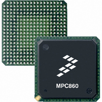
MPC855TCVR50D4 Freescale Semiconductor, MPC855TCVR50D4 Datasheet - Page 9

MPC855TCVR50D4
Manufacturer Part Number
MPC855TCVR50D4
Description
IC MPU POWERQUICC 50MHZ 357PBGA
Manufacturer
Freescale Semiconductor
Datasheets
1.MPC855TVR50D4.pdf
(15 pages)
2.MPC8555ECVTALF.pdf
(88 pages)
3.MPC855TCVR50D4.pdf
(80 pages)
Specifications of MPC855TCVR50D4
Processor Type
MPC8xx PowerQUICC 32-Bit
Speed
50MHz
Voltage
3.3V
Mounting Type
Surface Mount
Package / Case
357-PBGA
Processor Series
MPC8xx
Core
MPC8xx
Data Bus Width
32 bit
Maximum Clock Frequency
50 MHz
Operating Supply Voltage
2.5 V, 3.3 V
Maximum Operating Temperature
+ 95 C
Mounting Style
SMD/SMT
Minimum Operating Temperature
- 40 C
Family Name
MPC8xx
Device Core
PowerQUICC
Device Core Size
32b
Frequency (max)
50MHz
Instruction Set Architecture
RISC
Supply Voltage 1 (typ)
2.5/3.3V
Operating Supply Voltage (max)
3.465/3.6V
Operating Supply Voltage (min)
2/3.135V
Operating Temp Range
-40C to 95C
Operating Temperature Classification
Industrial
Mounting
Surface Mount
Pin Count
357
Package Type
BGA
Lead Free Status / RoHS Status
Lead free / RoHS Compliant
Features
-
Lead Free Status / Rohs Status
Lead free / RoHS Compliant
Available stocks
Company
Part Number
Manufacturer
Quantity
Price
Company:
Part Number:
MPC855TCVR50D4
Manufacturer:
FREESCAL
Quantity:
246
Company:
Part Number:
MPC855TCVR50D4
Manufacturer:
Freescale Semiconductor
Quantity:
10 000
Company:
Part Number:
MPC855TCVR50D4R2
Manufacturer:
Freescale Semiconductor
Quantity:
10 000
Independent transmit and receive buffer descriptor rings located in external memory allow nearly unlimited
flexibility in memory management of transmit and receive data frames. Locating buffer descriptors in
external memory has two advantages—first, external memory (i.e., DRAM) is low cost; secondly, descriptor
rings in external memory have no inherent size limitations, allowing the memory management to be
optimized according to specific system needs.
1.2.3
The SIU on the MPC855T integrates general-purpose features useful in almost any 32-bit processor system,
enhancing the performance provided by the system integration module (SIM) on the MC68360 QUICC
device.
Although the embedded MPC8xx core is always a 32-bit device internally, it may be configured to operate
with an 8-, 16- or 32-bit data bus. Regardless of the choice of the system bus size, dynamic bus sizing is
supported. Bus sizing allows 8-, 16-, and 32-bit peripherals and memory to exist in the 32-bit system bus
mode.
The SIU also provides power management functions, reset control, decrementer, time base and real-time
clock.
The memory controller supports up to eight memory banks with glueless interfaces to DRAM, SRAM,
SDRAM, EPROM, Flash EPROM, SRDRAM, EDO and other peripherals with two-clock access. The
memory controller supports bursting and variable memory block sizes from 32 Kbytes to 256 Mbytes. The
memory controller provides 0–15 wait states for each bank of memory and can use address type matching
to qualify each memory bank access. It also provides four byte-enable signals for varying width devices,
one output enable signal, and one boot chip select available at reset.
The DRAM interface supports port sizes of 8, 16, and 32 bits. Memory banks are defined in depths of 256
and 512 Kbytes, and 1, 2, 4, 8, 16, 32, and 64 Mbytes for all port sizes. In addition, memory depth is defined
as 64 Kbytes and 128 Kbytes for 8-bit memory or 128 Mbytes and 256 Mbytes for 32-bit memory. The
DRAM controller supports page mode access for successive transfers within bursts. The MPC855T supports
a glueless interface to one bank of DRAM; external buffers are required for additional memory banks. The
refresh unit provides CAS before RAS, a programmable refresh timer, refresh active during external reset,
disable refresh modes, and stacking up to seven refresh cycles. The DRAM interface uses a programmable
state machine to support almost any memory interface.PCMCIA Controller
The PCMCIA interface is a master (socket) controller and is compliant with release 2.1. The interface
supports up to two independent PCMCIA sockets requiring only external transceivers/buffers. The interface
provides eight memory or I/O windows where each window is allocated to a particular socket. If only one
PCMCIA port is being used, the unused PCMCIA port may be used as general-purpose input with interrupt
capability.
1.2.4
The MPC855T, like the earlier generation MPC850/860 family, implements a dual- processor architecture.
This dual-processor architecture provides both a high-performance, general-purpose processor for
application programming use as well as a special-purpose communications processor module (CPM)
uniquely designed for communications needs.
The CPM contains features that allow the 855T to excel in communications and networking products. These
features may be divided into three subgroups:
MOTOROLA
•
Communications processor (CP)
System Interface Unit (SIU)
Communications Processor Module (CPM)
MPC855T Communications Controller Technical Summary
Freescale Semiconductor, Inc.
For More Information On This Product,
Go to: www.freescale.com
MPC855T Architecture Overview
9


