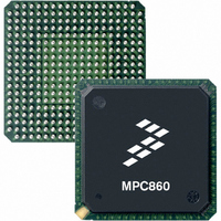
MPC855TCVR50D4 Freescale Semiconductor, MPC855TCVR50D4 Datasheet - Page 4

MPC855TCVR50D4
Manufacturer Part Number
MPC855TCVR50D4
Description
IC MPU POWERQUICC 50MHZ 357PBGA
Manufacturer
Freescale Semiconductor
Datasheets
1.MPC855TVR50D4.pdf
(15 pages)
2.MPC8555ECVTALF.pdf
(88 pages)
3.MPC855TCVR50D4.pdf
(80 pages)
Specifications of MPC855TCVR50D4
Processor Type
MPC8xx PowerQUICC 32-Bit
Speed
50MHz
Voltage
3.3V
Mounting Type
Surface Mount
Package / Case
357-PBGA
Processor Series
MPC8xx
Core
MPC8xx
Data Bus Width
32 bit
Maximum Clock Frequency
50 MHz
Operating Supply Voltage
2.5 V, 3.3 V
Maximum Operating Temperature
+ 95 C
Mounting Style
SMD/SMT
Minimum Operating Temperature
- 40 C
Family Name
MPC8xx
Device Core
PowerQUICC
Device Core Size
32b
Frequency (max)
50MHz
Instruction Set Architecture
RISC
Supply Voltage 1 (typ)
2.5/3.3V
Operating Supply Voltage (max)
3.465/3.6V
Operating Supply Voltage (min)
2/3.135V
Operating Temp Range
-40C to 95C
Operating Temperature Classification
Industrial
Mounting
Surface Mount
Pin Count
357
Package Type
BGA
Lead Free Status / RoHS Status
Lead free / RoHS Compliant
Features
-
Lead Free Status / Rohs Status
Lead free / RoHS Compliant
Available stocks
Company
Part Number
Manufacturer
Quantity
Price
Company:
Part Number:
MPC855TCVR50D4
Manufacturer:
FREESCAL
Quantity:
246
Company:
Part Number:
MPC855TCVR50D4
Manufacturer:
Freescale Semiconductor
Quantity:
10 000
Company:
Part Number:
MPC855TCVR50D4R2
Manufacturer:
Freescale Semiconductor
Quantity:
10 000
MPC855T Key Features
4
•
— Up to 32-bit data bus (dynamic bus sizing of 8, 16, and 32 bits provided through memory
— 32 address lines
System integration unit (SIU)
— Bus monitor
— Spurious interrupt monitor
— Software watchdog
— Periodic interrupt timer
— Low-power stop mode
— Clock synthesizer
— Decrementer
— Time base and RTC
— Reset controller
— IEEE 1149.1 test access port (JTAG)
— Memory controller (eight bank)
— General-purpose timers
fixed-point registers
– Embedded MPC8xx core performs branch folding and branch prediction with conditional
– 4-Kbyte data cache and 4-Kbyte instruction cache, each with an MMU
– Instruction and data caches are two-way, set associative, physical address, 4-word line
– MMUs with 32-entry, fully-associative instruction and data TLBs
– MMUs support multiple page sizes of 4 Kbytes, 16 Kbytes, 256 Kbytes, 512 Kbytes, and
– Advanced on-chip-emulation debug mode
controller)
– Contains complete dynamic random-access memory (DRAM) controller
– Each bank may be a chip select or RAS to support a DRAM bank
– Up to 15 wait states programmable per memory bank
– Glueless interface to DRAM single in-line memory modules (SIMMs), static
– DRAM controller programmable to support most size and speed memory interfaces
– Four CAS lines, four WE lines, one OE line
– Boot chip select available at reset (options for 8-, 16-, or 32-bit memory)
– Variable block sizes, 32 Kbytes to 256 Mbytes
– Selectable write protection
– On-chip bus arbitration logic
– Four 16-bit timers or two 32-bit timers
prefetch, but without conditional execution
burst, least recently used (LRU) replacement, lockable on cache line granularity
8 Kbytes; 16 virtual address spaces and 8 protection groups
random-access memory (SRAM), electrically programmable read-only memory
(EPROM), Flash EPROM, etc.
MPC855T Communications Controller Technical Summary
Freescale Semiconductor, Inc.
For More Information On This Product,
Go to: www.freescale.com
MOTOROLA


