CY7C68013-56PVC Cypress Semiconductor Corp, CY7C68013-56PVC Datasheet - Page 27
CY7C68013-56PVC
Manufacturer Part Number
CY7C68013-56PVC
Description
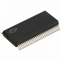
IC MCU USB PERIPH HI SPD 56SSOP
Manufacturer
Cypress Semiconductor Corp
Series
EZ-USB FX2LP™r
Datasheet
1.CY7C68013-56PVC.pdf
(52 pages)
Specifications of CY7C68013-56PVC
Applications
USB Microcontroller
Core Processor
8051
Program Memory Type
ROMless
Controller Series
CY7C680xx
Ram Size
16K x 8
Interface
I²C, USB, USART
Number Of I /o
24
Voltage - Supply
3 V ~ 3.6 V
Operating Temperature
0°C ~ 70°C
Mounting Type
Surface Mount
Package / Case
56-SSOP
Lead Free Status / RoHS Status
Contains lead / RoHS non-compliant
Other names
428-1332
Available stocks
Company
Part Number
Manufacturer
Quantity
Price
Company:

Part Number:
CY7C68013-56PVC
Manufacturer:
CY
Quantity:
5 530
Company:
Part Number:
CY7C68013-56PVC
Manufacturer:
CY
Quantity:
6 100
Part Number:
CY7C68013-56PVC
Manufacturer:
CYPRESS/赛普拉斯
Quantity:
20 000


Table 4-1. FX2 Pin Descriptions (continued)
Document #: 38-08012 Rev. *C
TQFP
PORT D
Port E
128
102
103
104
105
121
122
123
124
108
109
77
78
79
TQFP
100
62
63
64
80
81
82
83
95
96
97
98
86
87
SSOP
56
52
53
54
55
56
1
2
3
QFN
56
45 PD0 or
46 PD1 or
47 PD2 or
48 PD3 or
49 PD4 or
50 PD5 or
51 PD6 or
52 PD7 or
PC5 or
GPIFADR5
PC6 or
GPIFADR6
PC7 or
GPIFADR7
FD[8]
FD[9]
FD[10]
FD[11]
FD[12]
FD[13]
FD[14]
FD[15]
PE0 or
T0OUT
PE1 or
T1OUT
Name
Type
I/O/Z
I/O/Z
I/O/Z
I/O/Z
I/O/Z
I/O/Z
I/O/Z
I/O/Z
I/O/Z
I/O/Z
I/O/Z
I/O/Z
I/O/Z
[5]
Default
(PC5)
(PC6)
(PC7)
(PD0)
(PD1)
(PD2)
(PD3)
(PD4)
(PD5)
(PD6)
(PD7)
(PE0)
(PE1)
I
I
I
I
I
I
I
I
I
I
I
I
I
Multiplexed pin whose function is selected by PORTCCFG.5
PC5 is a bidirectional I/O port pin.
GPIFADR5 is a GPIF address output pin.
Multiplexed pin whose function is selected by PORTCCFG.6
PC6 is a bidirectional I/O port pin.
GPIFADR6 is a GPIF address output pin.
Multiplexed pin whose function is selected by PORTCCFG.7
PC7 is a bidirectional I/O port pin.
GPIFADR7 is a GPIF address output pin.
Multiplexed pin whose function is selected by the IFCONFIG[1..0]
and EPxFIFCFG.0 (wordwide) bits.
FD[8] is the bidirectional FIFO/GPIF data bus.
Multiplexed pin whose function is selected by the IFCONFIG[1..0]
and EPxFIFCFG.0 (wordwide) bits.
FD[9] is the bidirectional FIFO/GPIF data bus.
Multiplexed pin whose function is selected by the IFCONFIG[1..0]
and EPxFIFCFG.0 (wordwide) bits.
FD[10] is the bidirectional FIFO/GPIF data bus.
Multiplexed pin whose function is selected by the IFCONFIG[1..0]
and EPxFIFCFG.0 (wordwide) bits.
FD[11] is the bidirectional FIFO/GPIF data bus.
Multiplexed pin whose function is selected by the IFCONFIG[1..0]
and EPxFIFCFG.0 (wordwide) bits.
FD[12] is the bidirectional FIFO/GPIF data bus.
Multiplexed pin whose function is selected by the IFCONFIG[1..0]
and EPxFIFCFG.0 (wordwide) bits.
FD[13] is the bidirectional FIFO/GPIF data bus.
Multiplexed pin whose function is selected by the IFCONFIG[1..0]
and EPxFIFCFG.0 (wordwide) bits.
FD[14] is the bidirectional FIFO/GPIF data bus.
Multiplexed pin whose function is selected by the IFCONFIG[1..0]
and EPxFIFCFG.0 (wordwide) bits.
FD[15] is the bidirectional FIFO/GPIF data bus.
Multiplexed pin whose function is selected by the PORTECFG.0
bit.
PE0 is a bidirectional I/O port pin.
T0OUT is an active-HIGH signal from 8051 Timer-counter0.
T0OUT outputs a high level for one CLKOUT clock cycle when
Timer0 overflows. If Timer0 is operated in Mode 3 (two separate
timer/counters), T0OUT is active when the low byte timer/counter
overflows.
Multiplexed pin whose function is selected by the PORTECFG.1
bit.
PE1 is a bidirectional I/O port pin.
T1OUT is an active-HIGH signal from 8051 Timer-counter1.
T1OUT outputs a high level for one CLKOUT clock cycle when
Timer1 overflows. If Timer1 is operated in Mode 3 (two separate
timer/counters), T1OUT is active when the low byte timer/counter
overflows.
Description
CY7C68013
Page 27 of 52
Related parts for CY7C68013-56PVC
Image
Part Number
Description
Manufacturer
Datasheet
Request
R

Part Number:
Description:
IC MCU USB PERIPH HI SPD 100LQFP
Manufacturer:
Cypress Semiconductor Corp
Datasheet:

Part Number:
Description:
IC MCU USB PERIPH HI SPD 56SSOP
Manufacturer:
Cypress Semiconductor Corp
Datasheet:
Part Number:
Description:
IC MCU USB PERIPH HI SPD 100LQFP
Manufacturer:
Cypress Semiconductor Corp
Datasheet:

Part Number:
Description:
Manufacturer:
Cypress Semiconductor Corp
Datasheet:
Part Number:
Description:
Manufacturer:
Cypress Semiconductor Corp
Datasheet:

Part Number:
Description:
Manufacturer:
Cypress Semiconductor Corp
Datasheet:
Part Number:
Description:
Manufacturer:
Cypress Semiconductor Corp
Datasheet:
Part Number:
Description:
Manufacturer:
Cypress Semiconductor Corp
Datasheet:
Part Number:
Description:
Manufacturer:
Cypress Semiconductor Corp
Datasheet: