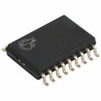
CY7C63231A-SC Cypress Semiconductor Corp, CY7C63231A-SC Datasheet - Page 22

CY7C63231A-SC
Manufacturer Part Number
CY7C63231A-SC
Description
IC MCU 3K USB LS PERIPH 18-SOIC
Manufacturer
Cypress Semiconductor Corp
Series
enCoRe™r
Datasheet
1.CY7C63231A-SXC.pdf
(50 pages)
Specifications of CY7C63231A-SC
Applications
USB Microcontroller
Core Processor
M8B
Program Memory Type
OTP (3 kB)
Controller Series
CY7C632xx
Ram Size
96 x 8
Interface
USB
Number Of I /o
10
Voltage - Supply
3.5 V ~ 5.5 V
Operating Temperature
0°C ~ 70°C
Mounting Type
Surface Mount
Package / Case
18-SOIC (7.5mm Width)
Operating Temperature (max)
70C
Operating Temperature (min)
0C
Operating Temperature Classification
Commercial
Package Type
SOIC
Mounting
Surface Mount
Lead Free Status / RoHS Status
Contains lead / RoHS non-compliant
Other names
428-1317
Available stocks
Company
Part Number
Manufacturer
Quantity
Price
Part Number:
CY7C63231A-SC
Manufacturer:
CYP
Quantity:
20 000
Bit [7:6]: Reserved
Bit [5:4]: D+ (SCLK) and D- (SDATA) States
Bit 3: Reserved
Bit 2: P2.2 (Internal Clock Mode Only)
Bit 1: P2.1 (Internal Clock Mode Only)
Bit 0: P2.0/ VREG Pin State
13.0
The SIE allows the microcontroller to communicate with the USB host. The SIE simplifies the interface between the microcon-
troller and USB by incorporating hardware that handles the following USB bus activity independently of the microcontroller:
Firmware is required to handle the rest of the USB interface with the following tasks:
Document #: 38-08028 Rev. *B
Read/Write
• Translate the encoded received data and format the data to be transmitted on the bus.
• CRC checking and generation. Flag the microcontroller if errors exist during transmission.
• Address checking. Ignore the transactions not addressed to the device.
• Send appropriate ACK/NAK/STALL handshakes.
• Token type identification (SETUP, IN, or OUT). Set the appropriate token bit once a valid token is received.
• Place valid received data in the appropriate endpoint FIFOs.
• Send and update the data toggle bit (Data1/0).
• Bit stuffing/unstuffing.
• Coordinate enumeration by decoding USB device requests.
• Fill and empty the FIFOs.
• Suspend/Resume coordination.
• Verify and select Data toggle values.
Bit Name
The state of the D+ and D– pins can be read at Port 2 Data Register. Performing a read from the port pins returns their logic
values.
1 = Port Pin is logic HIGH
0 = Port Pin is logic LOW
In the Internal Clock mode, the XTALOUT pin can serve as a general purpose input, and its state can be read at Port 2, Bit 2
(P2.2). See Section 9.1 for more details.
1 = Port Pin is logic HIGH
0 = Port Pin is logic LOW
In the Internal Clock mode, the XTALIN pin can serve as a general purpose input, and its state can be read at Port 2, Bit 1
(P2.1). See Section 9.1 for more details.
1 = Port Pin is logic HIGH
0 = Port Pin is logic LOW
In PS/2 mode, the VREG pin can be used as an input and its state can be read at port P2.0. Section 15.0 for more details.
1 = Port Pin is logic HIGH
0 = Port Pin is logic LOW
Reset
Bit #
USB Serial Interface Engine (SIE)
7
0
-
Reserved
6
0
-
Figure 12-8. Port 2 Data Register (Address 0x02)
FOR
FOR
D+ (SCLK)
State
R
5
0
D– (SDATA)
State
R
4
0
Reserved
3
0
-
Clock Mode
(Internal
Only)
P2.2
R
2
0
CY7C63221/31A
enCoRe™ USB
Clock Mode
(Internal
Only)
P2.1
R
1
0
Page 22 of 50
VREG Pin
State
P2.0
R
0
0
[+] Feedback


