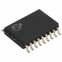
CY7C63231A-SC Cypress Semiconductor Corp, CY7C63231A-SC Datasheet - Page 19

CY7C63231A-SC
Manufacturer Part Number
CY7C63231A-SC
Description
IC MCU 3K USB LS PERIPH 18-SOIC
Manufacturer
Cypress Semiconductor Corp
Series
enCoRe™r
Datasheet
1.CY7C63231A-SXC.pdf
(50 pages)
Specifications of CY7C63231A-SC
Applications
USB Microcontroller
Core Processor
M8B
Program Memory Type
OTP (3 kB)
Controller Series
CY7C632xx
Ram Size
96 x 8
Interface
USB
Number Of I /o
10
Voltage - Supply
3.5 V ~ 5.5 V
Operating Temperature
0°C ~ 70°C
Mounting Type
Surface Mount
Package / Case
18-SOIC (7.5mm Width)
Operating Temperature (max)
70C
Operating Temperature (min)
0C
Operating Temperature Classification
Commercial
Package Type
SOIC
Mounting
Surface Mount
Lead Free Status / RoHS Status
Contains lead / RoHS non-compliant
Other names
428-1317
Available stocks
Company
Part Number
Manufacturer
Quantity
Price
Part Number:
CY7C63231A-SC
Manufacturer:
CYP
Quantity:
20 000
12.0
Ports 0 and 1 provide up to 10 versatile GPIO pins that can be read or written (the number of pins depends on package type).
Port 0 is an 8-bit port; Port 1 contains 2 bits, P1.1–P1.0 in the and CY7C63221A-XC parts. Each bit can also be selected as an
interrupt source for the microcontroller.
The data for each GPIO pin is accessible through the Port Data Register. Writes to the Port Data Register store outgoing data
state for the port pins, while reads from the Port Data Register return the actual logic value on the port pins, not the Port Data
Register contents.
Each GPIO pin is configured independently. The driving state of each GPIO pin is determined by the value written to the pin’s
Data Register and by two associated pin’s Mode0 and Mode1 bits.
The Port 0 Data Register is shown in Figure 12-2, and the Port 1 Data Register is shown in Figure 12-3. The Mode0 and Mode1
bits for the two GPIO ports are given in Figure 12-4 through Figure 12-7.
Bit [7:0]: P0[7:0]
Document #: 38-08028 Rev. *B
Read/Write
Bit Name
1 = Port Pin is logic HIGH
0 = Port Pin is logic LOW
Reset
Bit #
General Purpose I/O Ports
Internal
Data Bus
R/W
7
0
GPIO
Mode
Interrupt
Polarity
Interrupt
Enable
Port Write
Data
Out
Register
Figure 12-1. Block Diagram of GPIO Port (one pin shown)
R/W
6
0
Port Read
FOR
FOR
2
Figure 12-2. Port 0 Data (Address 0x00)
R/W
5
0
Interrupt
Logic
R/W
Threshold Select
4
0
P0
To Interrupt
Controller
R/W
Q1
Q2
3
0
14 kΩ
V
CC
Q3
R/W
2
0
CY7C63221/31A
enCoRe™ USB
GPIO
Pin
R/W
1
0
Page 19 of 50
R/W
0
0
[+] Feedback


