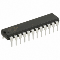
CY7C63743-PC Cypress Semiconductor Corp, CY7C63743-PC Datasheet - Page 20

CY7C63743-PC
Manufacturer Part Number
CY7C63743-PC
Description
IC MCU 8K LS USB/PS-2 24-DIP
Manufacturer
Cypress Semiconductor Corp
Series
enCoRe™r
Specifications of CY7C63743-PC
Applications
USB Microcontroller
Core Processor
M8B
Program Memory Type
OTP (8 kB)
Controller Series
CY7C637xx
Ram Size
256 x 8
Interface
PS2, USB
Number Of I /o
16
Voltage - Supply
4 V ~ 5.5 V
Operating Temperature
0°C ~ 70°C
Mounting Type
Through Hole
Package / Case
24-DIP (0.300", 7.62mm)
Lead Free Status / RoHS Status
Contains lead / RoHS non-compliant
Other names
428-1324
Available stocks
Company
Part Number
Manufacturer
Quantity
Price
Part Number:
CY7C63743-PC
Manufacturer:
CYPRESS/赛普拉斯
Quantity:
20 000
15.0
The VREG pin provides a regulated output for connecting the
pull-up resistor required for USB operation. For USB, a 1.5-kΩ
resistor is connected between the D– pin and the V
voltage, to indicate low-speed USB operation. Since the
VREG output has an internal series resistance of approxi-
mately 200Ω, the external pull-up resistor required is R
Section 25.0).
The regulator output is placed in a high-impedance state at
reset, and must be enabled by firmware by setting the VREG
Enable bit in the USB Status and Control Register
(Figure 13-1). This simplifies the design of a combination
PS/2-USB device, since the USB pull-up resistor can be left in
place during PS/2 operation without loading the PS/2 line. In
this mode, the V
can be read at port P2.0. Refer to Figure 12-8 for the Port 2
data register. This input has a TTL threshold.
In suspend mode, the regulator is automatically disabled. If
VREG Enable bit is set (Figure 13-1), the VREG pin is pulled
up to V
proper V
Note that enabling the device for USB (by setting the Device
Address Enable bit, Figure 14-1) activates the internal
regulator, even if the VREG Enable bit is cleared to 0. This
insures proper USB signaling in the case where the VREG pin
is used as an input, and an external regulator is provided for
the USB pull-up resistor. This also limits the swing on the D–
and D+ pins to about 1V above the internal regulator voltage,
so the Device Address Enable bit normally should only be set
for USB operating modes.
The regulator output is only designed to provide current for the
USB pull-up resistor. In addition, the output voltage at the
Document #: 38-08022 Rev. *B
CC
OH
USB Regulator Output
with an internal 6.2-kΩ resistor. This holds the
state in suspend mode
REG
pin can be used as an input and its state
VREG Enable
Port 2.5
Figure 16-1. Diagram of USB-PS/2 System Connections
Port 2.0
FOR
FOR
PS/2 Pull-up
Enable
Port 2.4
USB - PS/2
Driver
Regulator
3.3V
PU
(see
REG
5 kΩ
V
VREG pin is effectively disconnected when the CY7C637xx
device transmits USB from the internal SIE. This means that
the VREG pin does not provide a stable voltage during
transmits, although this does not affect USB signaling.
16.0
The CY7C637xx parts are optimized for combination USB or
PS/2 devices, through the following features:
The PS/2 on-chip support circuitry is illustrated in Figure 16-1.
1. USB D+ and D– lines can also be used for PS/2 SCLK and
2. An interrupt is provided to indicate a long LOW state on the
3. Internal PS/2 pull-up resistors can be enabled on the SCLK
4. The controlled slew rate outputs from these pins apply to
5. The state of the SCLK and SDATA pins can be read, and
6. The V
CC
SDATA pins, respectively. With USB disabled, these lines
can be placed in a high-impedance state that will pull up to
V
the USB Device Address Register, Figure 14-1).
SDATA pin. This eliminates the need to poll this pin to check
for PS/2 activity. Refer to Section 21.3 for more details.
and SDATA lines, so no GPIO pins are required for this task
(bit 7, USB Status and Control Register, Figure 13-1).
both USB and PS/2 modes to minimize EMI.
can be individually driven LOW in an open drain mode. The
pins are read at bits [5:4] of Port 2, and are driven with the
Control Bits [2:0] of the USB Status and Control Register.
so that a USB pull-up resistor on the D–/SDATA pin will not
interfere with PS/2 operation (bit 6, USB Status and Control
Register).
CC
5 kΩ
. (Disable USB by clearing the Address Enable bit of
REG
PS/2 Operation
200Ω
On-chip
pin can be placed into a high-impedance state,
Off-chip
VREG
1.3 kΩ
D+/SCLK
D–/SDATA
CY7C63722
CY7C63723
CY7C63743
Page 20 of 49


