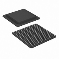
XC3S1200E-4FGG320I Xilinx Inc, XC3S1200E-4FGG320I Datasheet - Page 73

XC3S1200E-4FGG320I
Manufacturer Part Number
XC3S1200E-4FGG320I
Description
IC FPGA SPARTAN-3E 1200K 320FBGA
Manufacturer
Xilinx Inc
Series
Spartan™-3Er
Datasheet
1.XC3S100E-4VQG100C.pdf
(233 pages)
Specifications of XC3S1200E-4FGG320I
Number Of Logic Elements/cells
19512
Number Of Labs/clbs
2168
Total Ram Bits
516096
Number Of I /o
250
Number Of Gates
1200000
Voltage - Supply
1.14 V ~ 1.26 V
Mounting Type
Surface Mount
Operating Temperature
-40°C ~ 100°C
Package / Case
320-BGA
Lead Free Status / RoHS Status
Lead free / RoHS Compliant
Available stocks
Company
Part Number
Manufacturer
Quantity
Price
Company:
Part Number:
XC3S1200E-4FGG320I
Manufacturer:
Xilinx Inc
Quantity:
10 000
Part Number:
XC3S1200E-4FGG320I
Manufacturer:
XILINX/赛灵思
Quantity:
20 000
- Current page: 73 of 233
- Download datasheet (6Mb)
Table 50: Serial Master Mode Connections
DS312-2 (v3.8) August 26, 2009
Product Specification
Pin Name
HSWAP
M[2:0]
DIN
CCLK
DOUT
INIT_B
DONE
PROG_B
P
R
bidirectional
bidirectional
Open-drain
Open-drain
Direction
Output
Output
FPGA
Input
Input
Input
Input
I/O
I/O
User I/O Pull-Up Control. When Low during
configuration, enables pull-up resistors in all
I/O pins to respective I/O bank V
0: Pull-ups during configuration
1: No pull-ups
Mode Select. Selects the FPGA
configuration mode. See
Considerations for the HSWAP, M[2:0],
and VS[2:0]
Serial Data Input.
Configuration Clock. Generated by FPGA
internal oscillator. Frequency controlled by
ConfigRate bitstream generator option. If
CCLK PCB trace is long or has multiple
connections, terminate this output to
maintain signal integrity. See
Considerations.
Serial Data Output.
Initialization Indicator. Active Low. Goes
Low at start of configuration during
Initialization memory clearing process.
Released at end of memory clearing, when
mode select pins are sampled. Requires
external 4.7 kΩ pull-up resistor to VCCO_2.
FPGA Configuration Done. Low during
configuration. Goes High when FPGA
successfully completes configuration.
Requires external 330 Ω pull-up resistor to
2.5V.
Program FPGA. Active Low. When asserted
Low for 500 ns or longer, forces the FPGA to
restart its configuration process by clearing
configuration memory and resetting the
DONE and INIT_B pins once PROG_B
returns High. Recommend external 4.7 kΩ
pull-up resistor to 2.5V. Internal pull-up value
may be weaker (see
externally with a 3.3V output, use an
open-drain or open-collector driver or use a
current limiting series resistor.
Pins.
Description
Table
Design
78). If driving
CCLK Design
www.xilinx.com
CCO
input.
Drive at valid logic level
throughout configuration.
M2 = 0, M1 = 0, M0 = 0.
Sampled when INIT_B goes
High.
Receives serial data from
PROM’s D0 output.
Drives PROM’s CLK clock input.
Actively drives. Not used in
single-FPGA designs. In a
daisy-chain configuration, this pin
connects to DIN input of the next
FPGA in the chain.
Connects to PROM’s OE/RESET
input. FPGA clears PROM’s
address counter at start of
configuration, enables outputs
during configuration. PROM also
holds FPGA in Initialization state
until PROM reaches Power-On
Reset (POR) state. If CRC error
detected during configuration,
FPGA drives INIT_B Low.
Connects to PROM’s chip-enable
(CE) input. Enables PROM
during configuration. Disables
PROM after configuration.
Must be High during
configuration to allow
configuration to start. Connects
to PROM’s CF pin, allowing JTAG
PROM programming algorithm to
reprogram the FPGA.
During Configuration
Functional Description
User I/O
User I/O
User I/O
User I/O
User I/O
User I/O. If unused in
the application, drive
INIT_B High.
Pulled High via
external pull-up.
When High, indicates
that the FPGA
successfully
configured.
Drive PROG_B Low
and release to
reprogram FPGA.
After Configuration
73
Related parts for XC3S1200E-4FGG320I
Image
Part Number
Description
Manufacturer
Datasheet
Request
R

Part Number:
Description:
IC SPARTAN-3E FPGA 1200K 400FBGA
Manufacturer:
Xilinx Inc
Datasheet:

Part Number:
Description:
FPGA Spartan®-3E Family 1.2M Gates 19512 Cells 572MHz 90nm (CMOS) Technology 1.2V 256-Pin FTBGA
Manufacturer:
Xilinx Inc
Datasheet:

Part Number:
Description:
IC SPARTAN-3E FPGA 1200K 320FBGA
Manufacturer:
Xilinx Inc
Datasheet:

Part Number:
Description:
IC FPGA SPARTAN3E 1200K 256FTBGA
Manufacturer:
Xilinx Inc
Datasheet:

Part Number:
Description:
IC FPGA SPARTAN3E 1200K 256FTBGA
Manufacturer:
Xilinx Inc
Datasheet:

Part Number:
Description:
IC FPGA SPARTAN-3E 1200K 320FBGA
Manufacturer:
Xilinx Inc
Datasheet:

Part Number:
Description:
IC FPGA SPARTAN-3E 1200K 400FBGA
Manufacturer:
Xilinx Inc
Datasheet:

Part Number:
Description:
IC FPGA SPARTAN-3E 1200K 400FBGA
Manufacturer:
Xilinx Inc
Datasheet:

Part Number:
Description:
IC FPGA SPARTAN 3E 256FTBGA
Manufacturer:
Xilinx Inc
Datasheet:

Part Number:
Description:
IC FPGA SPARTAN 3E 320FBGA
Manufacturer:
Xilinx Inc
Datasheet:

Part Number:
Description:
PROGRAMMABLE INTEGRATED CIRCUIT
Manufacturer:
Xilinx Inc

Part Number:
Description:
FPGA Spartan®-3E Family 1.2M Gates 19512 Cells 572MHz 90nm (CMOS) Technology 1.2V 400-Pin FBGA
Manufacturer:
Xilinx Inc
Datasheet:

Part Number:
Description:
FPGA Spartan®-3E Family 1.2M Gates 19512 Cells 572MHz 90nm (CMOS) Technology 1.2V 256-Pin FTBGA
Manufacturer:
Xilinx Inc
Datasheet:

Part Number:
Description:
FPGA Spartan®-3E Family 1.2M Gates 19512 Cells 572MHz 90nm (CMOS) Technology 1.2V 320-Pin FBGA
Manufacturer:
Xilinx Inc
Datasheet:

Part Number:
Description:
IC CPLD .8K 36MCELL 44-VQFP
Manufacturer:
Xilinx Inc
Datasheet:


