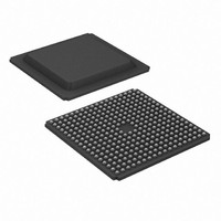
XC3S1200E-4FGG320I Xilinx Inc, XC3S1200E-4FGG320I Datasheet - Page 184

XC3S1200E-4FGG320I
Manufacturer Part Number
XC3S1200E-4FGG320I
Description
IC FPGA SPARTAN-3E 1200K 320FBGA
Manufacturer
Xilinx Inc
Series
Spartan™-3Er
Datasheet
1.XC3S100E-4VQG100C.pdf
(233 pages)
Specifications of XC3S1200E-4FGG320I
Number Of Logic Elements/cells
19512
Number Of Labs/clbs
2168
Total Ram Bits
516096
Number Of I /o
250
Number Of Gates
1200000
Voltage - Supply
1.14 V ~ 1.26 V
Mounting Type
Surface Mount
Operating Temperature
-40°C ~ 100°C
Package / Case
320-BGA
Lead Free Status / RoHS Status
Lead free / RoHS Compliant
Available stocks
Company
Part Number
Manufacturer
Quantity
Price
Company:
Part Number:
XC3S1200E-4FGG320I
Manufacturer:
Xilinx Inc
Quantity:
10 000
Part Number:
XC3S1200E-4FGG320I
Manufacturer:
XILINX/赛灵思
Quantity:
20 000
- Current page: 184 of 233
- Download datasheet (6Mb)
Pinout Descriptions
User I/Os by Bank
Table 138
user-I/O pins are distributed between the four I/O banks on
the TQ144 package.
Table 138: User I/Os Per Bank for the XC3S100E in the TQ144 Package
Table 139: User I/Os Per Bank for the XC3S250E in TQ144 Package
Footprint Migration Differences
Table 140
ences between the XC3S100E and the XC3S250E FPGAs
that may affect easy migration between devices. There are
four such pins. All other pins not listed in
ditionally migrate between Spartan-3E devices available in
the TQ144 package.
Table 140: TQ144 Footprint Migration Differences
184
Notes:
1.
2.
Notes:
1.
2.
Top
Right
Bottom
Left
TOTAL
Top
Right
Bottom
Left
TOTAL
Package
Package
TQ144 Pin
Some VREF and CLK pins are on INPUT pins.
The eight global clock pins in this bank have optional functionality during configuration and are counted in the DUAL column.
Some VREF and CLK pins are on INPUT pins.
The eight global clock pins in this bank have optional functionality during configuration and are counted in the DUAL column.
Edge
Edge
P10
P29
P31
P66
DIFFERENCES
summarizes any footprint and functionality differ-
and
Table 139
This pin can unconditionally migrate from the device on the left to the device on the right. Migration in the other direction may be
possible depending on how the pin is configured for the device on the right.
This pin can unconditionally migrate from the device on the right to the device on the left. Migration in the other direction may be
possible depending on how the pin is configured for the device on the left.
I/O Bank
I/O Bank
Bank
0
1
2
3
0
1
2
3
3
3
3
2
indicate how the 108 available
I/O
I/O
VREF(INPUT)
VREF(INPUT)
Maximum
Maximum
108
108
I/O
I/O
26
28
26
28
26
28
26
28
Table 140
XC3S100E Type
uncon-
I/O
I/O
11
20
13
22
9
0
0
9
0
0
www.xilinx.com
The arrows indicate the direction for easy migration. For
example, a left-facing arrow indicates that the pin on the
XC3S250E unconditionally migrates to the pin on the
XC3S100E. It may be possible to migrate the opposite
direction depending on the I/O configuration. For example,
an I/O pin (Type = I/O) can migrate to an input-only pin
(Type = INPUT) if the I/O pin is configured as an input.
INPUT
INPUT
21
19
6
5
4
6
6
5
4
4
All Possible I/O Pins by Type
All Possible I/O Pins by Type
Migration
4
DUAL
DUAL
21
20
42
21
20
42
1
0
1
0
DS312-4 (v3.8) August 26, 2009
VREF
VREF
2
2
2
3
9
2
2
2
3
9
XC3S250E Type
(1)
Product Specification
(1)
VREF(I/O)
VREF(I/O)
INPUT
INPUT
CLK
CLK
0
0
0
0
16
16
8
8
(2)
(2)
8
8
(1)
(1)
(1)
(1)
R
Related parts for XC3S1200E-4FGG320I
Image
Part Number
Description
Manufacturer
Datasheet
Request
R

Part Number:
Description:
IC SPARTAN-3E FPGA 1200K 400FBGA
Manufacturer:
Xilinx Inc
Datasheet:

Part Number:
Description:
FPGA Spartan®-3E Family 1.2M Gates 19512 Cells 572MHz 90nm (CMOS) Technology 1.2V 256-Pin FTBGA
Manufacturer:
Xilinx Inc
Datasheet:

Part Number:
Description:
IC SPARTAN-3E FPGA 1200K 320FBGA
Manufacturer:
Xilinx Inc
Datasheet:

Part Number:
Description:
IC FPGA SPARTAN3E 1200K 256FTBGA
Manufacturer:
Xilinx Inc
Datasheet:

Part Number:
Description:
IC FPGA SPARTAN3E 1200K 256FTBGA
Manufacturer:
Xilinx Inc
Datasheet:

Part Number:
Description:
IC FPGA SPARTAN-3E 1200K 320FBGA
Manufacturer:
Xilinx Inc
Datasheet:

Part Number:
Description:
IC FPGA SPARTAN-3E 1200K 400FBGA
Manufacturer:
Xilinx Inc
Datasheet:

Part Number:
Description:
IC FPGA SPARTAN-3E 1200K 400FBGA
Manufacturer:
Xilinx Inc
Datasheet:

Part Number:
Description:
IC FPGA SPARTAN 3E 256FTBGA
Manufacturer:
Xilinx Inc
Datasheet:

Part Number:
Description:
IC FPGA SPARTAN 3E 320FBGA
Manufacturer:
Xilinx Inc
Datasheet:

Part Number:
Description:
PROGRAMMABLE INTEGRATED CIRCUIT
Manufacturer:
Xilinx Inc

Part Number:
Description:
FPGA Spartan®-3E Family 1.2M Gates 19512 Cells 572MHz 90nm (CMOS) Technology 1.2V 400-Pin FBGA
Manufacturer:
Xilinx Inc
Datasheet:

Part Number:
Description:
FPGA Spartan®-3E Family 1.2M Gates 19512 Cells 572MHz 90nm (CMOS) Technology 1.2V 256-Pin FTBGA
Manufacturer:
Xilinx Inc
Datasheet:

Part Number:
Description:
FPGA Spartan®-3E Family 1.2M Gates 19512 Cells 572MHz 90nm (CMOS) Technology 1.2V 320-Pin FBGA
Manufacturer:
Xilinx Inc
Datasheet:

Part Number:
Description:
IC CPLD .8K 36MCELL 44-VQFP
Manufacturer:
Xilinx Inc
Datasheet:


