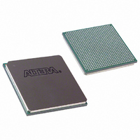
EP1S25F780C6 Altera, EP1S25F780C6 Datasheet - Page 160

EP1S25F780C6
Manufacturer Part Number
EP1S25F780C6
Description
IC STRATIX FPGA 25K LE 780-FBGA
Manufacturer
Altera
Series
Stratix®r
Datasheet
1.EP1S10F780C7.pdf
(276 pages)
Specifications of EP1S25F780C6
Number Of Logic Elements/cells
25660
Number Of Labs/clbs
2566
Total Ram Bits
1944576
Number Of I /o
597
Voltage - Supply
1.425 V ~ 1.575 V
Mounting Type
Surface Mount
Operating Temperature
0°C ~ 85°C
Package / Case
780-FBGA
Family Name
Stratix
Number Of Logic Blocks/elements
25660
# I/os (max)
597
Frequency (max)
450.05MHz
Process Technology
0.13um (CMOS)
Operating Supply Voltage (typ)
1.5V
Logic Cells
25660
Ram Bits
1944576
Operating Supply Voltage (min)
1.425V
Operating Supply Voltage (max)
1.575V
Operating Temp Range
0C to 85C
Operating Temperature Classification
Commercial
Mounting
Surface Mount
Pin Count
780
Package Type
FC-FBGA
Lead Free Status / RoHS Status
Contains lead / RoHS non-compliant
Number Of Gates
-
Lead Free Status / Rohs Status
Not Compliant
Other names
544-1121
Available stocks
Company
Part Number
Manufacturer
Quantity
Price
Company:
Part Number:
EP1S25F780C6
Manufacturer:
ALTERA
Quantity:
10
Company:
Part Number:
EP1S25F780C6
Manufacturer:
ALTERA
Quantity:
246
Part Number:
EP1S25F780C6
Manufacturer:
ALTERA/阿尔特拉
Quantity:
20 000
Part Number:
EP1S25F780C6ES
Manufacturer:
ALTERA
Quantity:
20 000
Company:
Part Number:
EP1S25F780C6N
Manufacturer:
ALTERA
Quantity:
1 045
Configuration
3–6
Stratix Device Handbook, Volume 1
configuration, the device resets registers, enables I/O pins, and begins to
operate as a logic device. The I/O pins are tri-stated during power-up,
and before and during configuration. Together, the configuration and
initialization processes are called command mode. Normal device
operation is called user mode.
SRAM configuration elements allow Stratix devices to be reconfigured in-
circuit by loading new configuration data into the device. With real-time
reconfiguration, the device is forced into command mode with a device
pin. The configuration process loads different configuration data,
reinitializes the device, and resumes user-mode operation. You can
perform in-field upgrades by distributing new configuration files either
within the system or remotely.
PORSEL is a dedicated input pin used to select POR delay times of 2 ms
or 100 ms during power-up. When the PORSEL pin is connected to
ground, the POR time is 100 ms; when the PORSEL pin is connected to
V
The nIO_PULLUP pin enables a built-in weak pull-up resistor to pull all
user I/O pins to V
nIO_PULLUP is connected to V
ups on all user I/O pins are disabled. If connected to ground, the pull-ups
are enabled during configuration. The nIO_PULLUP pin can be pulled to
1.5, 1.8, 2.5, or 3.3 V for a logic level high.
VCCSEL is a dedicated input that is used to choose whether all dedicated
configuration and JTAG input pins can accept 1.5 V/1.8 V or 2.5 V/3.3 V
during configuration. A logic low sets 3.3 V/2.5 V, and a logic high sets
1.8 V/1.5 V. VCCSEL affects the following pins: TDI, TMS, TCK, TRST,
MSEL0, MSEL1, MSEL2, nCONFIG, nCE, DCLK, PLL_ENA, CONF_DONE,
nSTATUS. The VCCSEL pin can be pulled to 1.5, 1.8, 2.5, or 3.3 V for a logic
level high.
The VCCSEL signal does not control the dual-purpose configuration pins
such as the DATA[7..0] and PPA pins (nWS, nRS, CS, nCS, and
RDYnBSY). During configuration, these dual-purpose pins will drive out
voltage levels corresponding to the V
I/O bank containing the pin. After configuration, the dual-purpose pins
use I/O standards specified in the user design.
TDO and nCEO drive out at the same voltages as the V
powers the I/O bank containing the pin. Users must select the V
supply for bank containing TDO accordingly. For example, when using
the ByteBlaster
be powered up at 3.3 V.
CC
, the POR time is 2 ms.
™
MV cable, the V
CCIO
before and during device configuration. If
CC
CCIO
during configuration, the weak pull-
CCIO
for the bank containing TDO must
supply voltage that powers the
CCIO
Altera Corporation
supply that
July 2005
CCIO


