EP3C5E144I7 Altera, EP3C5E144I7 Datasheet - Page 6
EP3C5E144I7
Manufacturer Part Number
EP3C5E144I7
Description
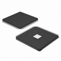
IC CYCLONE III FPGA 5K 144 EQFP
Manufacturer
Altera
Series
Cyclone® IIIr
Datasheets
1.EP3C5F256C8N.pdf
(5 pages)
2.EP3C5F256C8N.pdf
(34 pages)
3.EP3C5F256C8N.pdf
(66 pages)
4.EP3C5F256C8N.pdf
(14 pages)
5.EP3C5F256C8N.pdf
(76 pages)
Specifications of EP3C5E144I7
Number Of Logic Elements/cells
5136
Number Of Labs/clbs
321
Total Ram Bits
423936
Number Of I /o
94
Voltage - Supply
1.15 V ~ 1.25 V
Mounting Type
Surface Mount
Operating Temperature
-40°C ~ 100°C
Package / Case
144-EQFP
Lead Free Status / RoHS Status
Contains lead / RoHS non-compliant
Number Of Gates
-
Available stocks
Company
Part Number
Manufacturer
Quantity
Price

Company:
Part Number:
EP3C5E144I7N
Manufacturer:
Altera
Quantity:
135
Company:
Part Number:
EP3C5E144I7N
Manufacturer:
ALTERA32
Quantity:
345
Part Number:
EP3C5E144I7N
Manufacturer:
ALTERA/阿尔特拉
Quantity:
20 000


Page 6
Planning and Selecting Configuration Scheme
f
f
f
f
f
External Memory Interface
Cyclone III devices support interfaces to the DDR2 SDRAM, DDR SDRAM, and
QDRII SRAM. Depending on device density and package, specific side of I/O bank
may support up to ×36 mode of memory interface. Supported modes in the
Cyclone III devices are ×8, ×9, ×16, ×18, ×32, and ×36 modes. Use the Pin Planner tool
to assist you in determining and making pin assignments for the memory interface.
In general, choose the top or bottom I/O banks instead of the side I/O banks to
achieve a higher clock rate for the external memory interfaces. The Cyclone III devices
support external memory interfaces up to 200 MHz.
For more information about the DDR/DDR2 and QDRII pads placement, refer to the
Cyclone III Device I/O Feature
For more information about the recommended design flow to implement the
DDR2 SDRAM memory interface with Cyclone III devices, refer to
Guidelines for Implementing DDR and DDR2 SDRAM Interfaces in Cyclone III Devices.
For a complete table of the maximum clock rate support across all speed grades for
every memory standard, refer to the
the Cyclone III Device Handbook.
Pin-Out Files
The Cyclone III pin-out files contain information about the location for all the pins of
the devices, according to package. For the I/O pins, you can also know which I/O
bank and the V
description for the dedicated and multi-purpose pins. The pin-out files help designer
to determine the I/O pins to be used when creating the design as well as when
designing the board. Apart from I/O pins, the location of dedicated and
multi-purpose pins is also important during the board design stage.
To obtain device pin-outs for Cyclone III devices, refer to the
the Literature section of the Altera website (www.altera.com).
Choose your device configuration method early to allow system and board designers
to determine if any additional devices are required for your system. Your board layout
depends on the configuration method that you plan to use for the programmable
device, because different schemes require different connections.
For board design guidelines related to configuration pins, refer to
Considerations”.
REF
group the pins belong to. The pin-out files also contain the
chapter in volume 1 of the Cyclone III Device Handbook.
External Memory Interfaces
© November 2008 Altera Corporation
Device Pin-Outs
chapter in volume 1 of
“Board Design
AN 445: Design
Early System Planning
page of
Related parts for EP3C5E144I7
Image
Part Number
Description
Manufacturer
Datasheet
Request
R

Part Number:
Description:
CYCLONE II STARTER KIT EP2C20N
Manufacturer:
Altera
Datasheet:


Part Number:
Description:
CPLD, EP610 Family, ECMOS Process, 300 Gates, 16 Macro Cells, 16 Reg., 16 User I/Os, 5V Supply, 35 Speed Grade, 24DIP
Manufacturer:
Altera Corporation
Datasheet:
Part Number:
Description:
CPLD, EP610 Family, ECMOS Process, 300 Gates, 16 Macro Cells, 16 Reg., 16 User I/Os, 5V Supply, 15 Speed Grade, 24DIP
Manufacturer:
Altera Corporation
Datasheet:
Part Number:
Description:
Manufacturer:
Altera Corporation
Datasheet:
Part Number:
Description:
CPLD, EP610 Family, ECMOS Process, 300 Gates, 16 Macro Cells, 16 Reg., 16 User I/Os, 5V Supply, 30 Speed Grade, 24DIP
Manufacturer:
Altera Corporation
Datasheet:
Part Number:
Description:
High-performance, low-power erasable programmable logic devices with 8 macrocells, 10ns
Manufacturer:
Altera Corporation
Datasheet:
Part Number:
Description:
High-performance, low-power erasable programmable logic devices with 8 macrocells, 7ns
Manufacturer:
Altera Corporation
Datasheet:
Part Number:
Description:
Classic EPLD
Manufacturer:
Altera Corporation
Datasheet:
Part Number:
Description:
High-performance, low-power erasable programmable logic devices with 8 macrocells, 10ns
Manufacturer:
Altera Corporation
Datasheet:
Part Number:
Description:
Manufacturer:
Altera Corporation
Datasheet:
Part Number:
Description:
Manufacturer:
Altera Corporation
Datasheet:
Part Number:
Description:
Manufacturer:
Altera Corporation
Datasheet:
Part Number:
Description:
CPLD, EP610 Family, ECMOS Process, 300 Gates, 16 Macro Cells, 16 Reg., 16 User I/Os, 5V Supply, 25 Speed Grade, 24DIP
Manufacturer:
Altera Corporation
Datasheet: