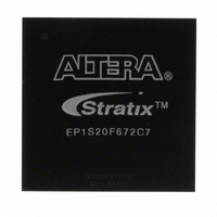
EP1S20F672C7 Altera, EP1S20F672C7 Datasheet - Page 48

EP1S20F672C7
Manufacturer Part Number
EP1S20F672C7
Description
IC STRATIX FPGA 20K LE 672-FBGA
Manufacturer
Altera
Series
Stratix®r
Datasheet
1.EP1S10F780C7.pdf
(276 pages)
Specifications of EP1S20F672C7
Number Of Logic Elements/cells
18460
Number Of Labs/clbs
1846
Total Ram Bits
1669248
Number Of I /o
426
Voltage - Supply
1.425 V ~ 1.575 V
Mounting Type
Surface Mount
Operating Temperature
0°C ~ 85°C
Package / Case
672-FBGA
Family Name
Stratix
Number Of Logic Blocks/elements
18460
# I/os (max)
426
Frequency (max)
420.17MHz
Process Technology
0.13um (CMOS)
Operating Supply Voltage (typ)
1.5V
Logic Cells
18460
Ram Bits
1669248
Operating Supply Voltage (min)
1.425V
Operating Supply Voltage (max)
1.575V
Operating Temp Range
0C to 85C
Operating Temperature Classification
Commercial
Mounting
Surface Mount
Pin Count
672
Package Type
FBGA
Lead Free Status / RoHS Status
Contains lead / RoHS non-compliant
Number Of Gates
-
Lead Free Status / Rohs Status
Not Compliant
Other names
544-1113
Available stocks
Company
Part Number
Manufacturer
Quantity
Price
Company:
Part Number:
EP1S20F672C7
Manufacturer:
SHARP
Quantity:
3 509
Company:
Part Number:
EP1S20F672C7
Manufacturer:
ALTERA
Quantity:
528
Part Number:
EP1S20F672C7
Manufacturer:
ALTERA/阿尔特拉
Quantity:
20 000
Company:
Part Number:
EP1S20F672C7N
Manufacturer:
Harting
Quantity:
1 000
Company:
Part Number:
EP1S20F672C7N
Manufacturer:
ALTERA
Quantity:
3 000
TriMatrix Memory
2–34
Stratix Device Handbook, Volume 1
M-RAM Block
The largest TriMatrix memory block, the M-RAM block, is useful for
applications where a large volume of data must be stored on-chip. Each
block contains 589,824 RAM bits (including parity bits). The M-RAM
block can be configured in the following modes:
■
■
■
■
You cannot use an initialization file to initialize the contents of a M-RAM
block. All M-RAM block contents power up to an undefined value. Only
synchronous operation is supported in the M-RAM block, so all inputs
are registered. Output registers can be bypassed. The memory address
and output width can be configured as 64K × 8 (or 64K × 9 bits), 32K × 16
(or 32K × 18 bits), 16K × 32 (or 16K × 36 bits), 8K × 64 (or 8K × 72 bits), and
4K × 128 (or 4K × 144 bits). The 4K × 128 configuration is unavailable in
true dual-port mode because there are a total of 144 data output drivers
in the block. Mixed-width configurations are also possible, allowing
different read and write widths.
possible M-RAM block configurations:
64K
32K
16K
8K
4K
Table 2–8. M-RAM Block Configurations (Simple Dual-Port)
Read Port
×
×
True dual-port RAM
Simple dual-port RAM
Single-port RAM
FIFO RAM
×
×
×
72
144
9
18
36
64K × 9
v
v
v
v
32K × 18
v
v
v
v
Tables 2–8
Write Port
16K × 36
v
v
v
v
and
2–9
summarize the
8K × 72
v
v
v
v
Altera Corporation
4K × 144
July 2005
v


