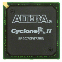
EP2C70F672I8N Altera, EP2C70F672I8N Datasheet - Page 55

EP2C70F672I8N
Manufacturer Part Number
EP2C70F672I8N
Description
IC CYCLONE II FPGA 70K 672-FBGA
Manufacturer
Altera
Series
Cyclone® IIr
Datasheet
1.EP2C5T144C8N.pdf
(168 pages)
Specifications of EP2C70F672I8N
Number Of Logic Elements/cells
68416
Number Of Labs/clbs
4276
Total Ram Bits
1152000
Number Of I /o
422
Voltage - Supply
1.15 V ~ 1.25 V
Mounting Type
Surface Mount
Operating Temperature
-40°C ~ 100°C
Package / Case
672-FBGA
Family Name
Cyclone® II
Number Of Logic Blocks/elements
68416
# I/os (max)
422
Frequency (max)
402.58MHz
Process Technology
90nm
Operating Supply Voltage (typ)
1.2V
Logic Cells
68416
Ram Bits
1152000
Operating Supply Voltage (min)
1.15V
Operating Supply Voltage (max)
1.25V
Operating Temp Range
-40C to 100C
Operating Temperature Classification
Industrial
Mounting
Surface Mount
Pin Count
672
Package Type
FBGA
For Use With
P0304 - DE2-70 CALL FOR ACADEMIC PRICING544-1703 - VIDEO KIT W/CYCLONE II EP2C70N544-1699 - DSP KIT W/CYCLONE II EPS2C70N
Lead Free Status / RoHS Status
Lead free / RoHS Compliant
Number Of Gates
-
Lead Free Status / Rohs Status
Compliant
Other names
544-2143
Available stocks
Company
Part Number
Manufacturer
Quantity
Price
Company:
Part Number:
EP2C70F672I8N
Manufacturer:
ALTERA
Quantity:
490
Part Number:
EP2C70F672I8N
Manufacturer:
BGA
Quantity:
20 000
Figure 2–25. Cyclone II IOE in Bidirectional I/O Configuration
Altera Corporation
February 2007
Interconect
Column
or Row
io_clk[5..0]
data_in1
data_in0
Chip-Wide Reset
OE
clkout
aclr/prn
ce_in
ce_out
clkin
sclr/preset
The Cyclone II device IOE includes programmable delays to ensure zero
hold times, minimize setup times, or increase clock to output times.
A path in which a pin directly drives a register may require a
programmable delay to ensure zero hold time, whereas a path in which a
pin drives a register through combinational logic may not require the
delay. Programmable delays decrease input-pin-to-logic-array and IOE
input register delays. The Quartus II Compiler can program these delays
to automatically minimize setup time while providing a zero hold time.
Output Register
Input Register
OE Register
D
D
D
CLRN
CLRN
CLRN
PRN
ENA
PRN
ENA
PRN
ENA
Q
Q
Q
Pin Delay
Open-Drain Output
Output
Cyclone II Device Handbook, Volume 1
Input Register Delay
Logic Array Delay
or Input Pin to
Input Pin to
Cyclone II Architecture
V
CCIO
V
CCIO
Optional
PCI Clamp
Programmable
Pull-Up
Resistor
Bus Hold
2–43


