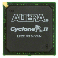
EP2C70F672I8N Altera, EP2C70F672I8N Datasheet - Page 32

EP2C70F672I8N
Manufacturer Part Number
EP2C70F672I8N
Description
IC CYCLONE II FPGA 70K 672-FBGA
Manufacturer
Altera
Series
Cyclone® IIr
Datasheet
1.EP2C5T144C8N.pdf
(168 pages)
Specifications of EP2C70F672I8N
Number Of Logic Elements/cells
68416
Number Of Labs/clbs
4276
Total Ram Bits
1152000
Number Of I /o
422
Voltage - Supply
1.15 V ~ 1.25 V
Mounting Type
Surface Mount
Operating Temperature
-40°C ~ 100°C
Package / Case
672-FBGA
Family Name
Cyclone® II
Number Of Logic Blocks/elements
68416
# I/os (max)
422
Frequency (max)
402.58MHz
Process Technology
90nm
Operating Supply Voltage (typ)
1.2V
Logic Cells
68416
Ram Bits
1152000
Operating Supply Voltage (min)
1.15V
Operating Supply Voltage (max)
1.25V
Operating Temp Range
-40C to 100C
Operating Temperature Classification
Industrial
Mounting
Surface Mount
Pin Count
672
Package Type
FBGA
For Use With
P0304 - DE2-70 CALL FOR ACADEMIC PRICING544-1703 - VIDEO KIT W/CYCLONE II EP2C70N544-1699 - DSP KIT W/CYCLONE II EPS2C70N
Lead Free Status / RoHS Status
Lead free / RoHS Compliant
Number Of Gates
-
Lead Free Status / Rohs Status
Compliant
Other names
544-2143
Available stocks
Company
Part Number
Manufacturer
Quantity
Price
Company:
Part Number:
EP2C70F672I8N
Manufacturer:
ALTERA
Quantity:
490
Part Number:
EP2C70F672I8N
Manufacturer:
BGA
Quantity:
20 000
Global Clock Network & Phase-Locked Loops
2–20
Cyclone II Device Handbook, Volume 1
Dedicated Clock Pins
Larger Cyclone II devices (EP2C15 and larger devices) have 16 dedicated
clock pins (CLK[15..0], four pins on each side of the device). Smaller
Cyclone II devices (EP2C5 and EP2C8 devices) have eight dedicated clock
pins (CLK[7..0], four pins on left and right sides of the device). These
CLK pins drive the global clock network (GCLK), as shown in
Figures 2–11
If the dedicated clock pins are not used to feed the global clock networks,
they can be used as general-purpose input pins to feed the logic array
using the MultiTrack interconnect. However, if they are used as general-
purpose input pins, they do not have support for an I/O register and
must use LE-based registers in place of an I/O register.
Dual-Purpose Clock Pins
Cyclone II devices have either 20 dual-purpose clock pins,
DPCLK[19..0] or 8 dual-purpose clock pins, DPCLK[7..0]. In the
larger Cyclone II devices (EP2C15 devices and higher), there are
20 DPCLK pins; four on the left and right sides and six on the top and
bottom of the device. The corner CDPCLK pins are first multiplexed before
they drive into the clock control block. Since the signals pass through a
multiplexer before feeding the clock control block, these signals incur
more delay to the clock control block than other DPCLK pins that directly
feed the clock control block. In the smaller Cyclone II devices (EP2C5 and
EP2C8 devices), there are eight DPCLK pins; two on each side of the device
(see
A programmable delay chain is available from the DPCLK pin to its fan-
out destinations. To set the propagation delay from the DPCLK pin to its
fan-out destinations, use the Input Delay from Dual-Purpose Clock Pin
to Fan-Out Destinations assignment in the Quartus II software.
These dual-purpose pins can connect to the global clock network for
high-fanout control signals such as clocks, asynchronous clears, presets,
and clock enables, or protocol control signals such as TRDY and IRDY for
PCI, or DQS signals for external memory interfaces.
Figures 2–11
and 2–12.
and 2–12).
Altera Corporation
February 2007


