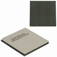
EP1AGX90EF1152C6N Altera, EP1AGX90EF1152C6N Datasheet - Page 26

EP1AGX90EF1152C6N
Manufacturer Part Number
EP1AGX90EF1152C6N
Description
IC ARRIA GX FPGA 90K 1152FBGA
Manufacturer
Altera
Series
Arria GXr
Datasheet
1.EP1AGX20CF484C6N.pdf
(234 pages)
Specifications of EP1AGX90EF1152C6N
Number Of Logic Elements/cells
90220
Number Of Labs/clbs
4511
Total Ram Bits
4477824
Number Of I /o
538
Voltage - Supply
1.15 V ~ 1.25 V
Mounting Type
Surface Mount
Operating Temperature
0°C ~ 85°C
Package / Case
1152-FBGA
Lead Free Status / RoHS Status
Lead free / RoHS Compliant
Number Of Gates
-
Other names
544-2379
Available stocks
Company
Part Number
Manufacturer
Quantity
Price
Company:
Part Number:
EP1AGX90EF1152C6N
Manufacturer:
ALTERA
Quantity:
3 000
- Current page: 26 of 234
- Download datasheet (4Mb)
2–20
Loopback Modes
Figure 2–18. Transceiver Data Path in Serial Loopback
Arria GX Device Handbook, Volume 1
PLD
Logic
Array
f
f
Byte Deserializer
Byte deserializer takes in one-byte wide data from the 8B/10B decoder and
deserializes it into a two-byte wide data at half the speed. This allows clocking the
PLD-receiver interface at half the speed as compared to the receiver PCS logic. The
byte deserializer is bypassed in GIGE mode.
The byte ordering at the receiver output might be different than what was
transmitted. This is a non-deterministic swap, because it depends on PLL lock times
and link delay. If required, you must implement byte ordering logic in the PLD to
correct this situation.
For more information about byte serializer, refer to the
Architecture
Receiver Phase Compensation FIFO Buffer
A receiver phase compensation FIFO buffer is located at each receiver channel’s logic
array interface. It compensates for the phase difference between the receiver PCS
clock and the local PLD receiver clock. The receiver phase compensation FIFO is used
in all supported functional modes. The receiver phase compensation FIFO buffer is
eight words deep in PCI Express (PIPE) mode and four words deep in all other
modes.
For more information about architecture and clocking, refer to the
Architecture
Arria GX transceivers support the following loopback configurations for diagnostic
purposes:
■
■
■
■
Serial Loopback
Figure 2–18
RX Phase
Compen-
sation
Serial loopback
Reverse serial loopback
Reverse serial loopback (pre-CDR)
PCI Express (PIPE) reverse parallel loopback (available only in [PIPE] mode)
FIFO
TX Phase
Compen-
sation
FIFO
chapter.
chapter.
shows the transceiver data path in serial loopback.
Serializer
Byte
De-
Serializer
Byte
Decoder
8B/10B
Encoder
8B/10B
Match
FIFO
Rate
Transmitter PCS
Receiver PCS
Aligner
Word
Arria GX Transceiver
Receiver PMA
Serializer
© December 2009 Altera Corporation
De-
Transmitter PMA
Serial Loopback
Chapter 2: Arria GX Architecture
Serializer
Recovery
Clock
Unit
Arria GX Transceiver
Transceivers
Related parts for EP1AGX90EF1152C6N
Image
Part Number
Description
Manufacturer
Datasheet
Request
R

Part Number:
Description:
CYCLONE II STARTER KIT EP2C20N
Manufacturer:
Altera
Datasheet:

Part Number:
Description:
CPLD, EP610 Family, ECMOS Process, 300 Gates, 16 Macro Cells, 16 Reg., 16 User I/Os, 5V Supply, 35 Speed Grade, 24DIP
Manufacturer:
Altera Corporation
Datasheet:

Part Number:
Description:
CPLD, EP610 Family, ECMOS Process, 300 Gates, 16 Macro Cells, 16 Reg., 16 User I/Os, 5V Supply, 15 Speed Grade, 24DIP
Manufacturer:
Altera Corporation
Datasheet:

Part Number:
Description:
Manufacturer:
Altera Corporation
Datasheet:

Part Number:
Description:
CPLD, EP610 Family, ECMOS Process, 300 Gates, 16 Macro Cells, 16 Reg., 16 User I/Os, 5V Supply, 30 Speed Grade, 24DIP
Manufacturer:
Altera Corporation
Datasheet:

Part Number:
Description:
High-performance, low-power erasable programmable logic devices with 8 macrocells, 10ns
Manufacturer:
Altera Corporation
Datasheet:

Part Number:
Description:
High-performance, low-power erasable programmable logic devices with 8 macrocells, 7ns
Manufacturer:
Altera Corporation
Datasheet:

Part Number:
Description:
Classic EPLD
Manufacturer:
Altera Corporation
Datasheet:

Part Number:
Description:
High-performance, low-power erasable programmable logic devices with 8 macrocells, 10ns
Manufacturer:
Altera Corporation
Datasheet:

Part Number:
Description:
Manufacturer:
Altera Corporation
Datasheet:

Part Number:
Description:
Manufacturer:
Altera Corporation
Datasheet:

Part Number:
Description:
Manufacturer:
Altera Corporation
Datasheet:

Part Number:
Description:
CPLD, EP610 Family, ECMOS Process, 300 Gates, 16 Macro Cells, 16 Reg., 16 User I/Os, 5V Supply, 25 Speed Grade, 24DIP
Manufacturer:
Altera Corporation
Datasheet:


