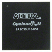
EP2C35U484C6 Altera, EP2C35U484C6 Datasheet - Page 95

EP2C35U484C6
Manufacturer Part Number
EP2C35U484C6
Description
IC CYCLONE II FPGA 33K 484-UBGA
Manufacturer
Altera
Series
Cyclone® IIr
Datasheet
1.EP2C5T144C8N.pdf
(168 pages)
Specifications of EP2C35U484C6
Number Of Logic Elements/cells
33216
Number Of Labs/clbs
2076
Total Ram Bits
483840
Number Of I /o
322
Voltage - Supply
1.15 V ~ 1.25 V
Mounting Type
Surface Mount
Operating Temperature
0°C ~ 85°C
Package / Case
484-UBGA
For Use With
P0301 - DE2 CALL FOR ACADEMIC PRICING544-1733 - PCI KIT W/CYCLONE II EP2C35N
Lead Free Status / RoHS Status
Contains lead / RoHS non-compliant
Number Of Gates
-
Other names
544-2112
Available stocks
Company
Part Number
Manufacturer
Quantity
Price
Company:
Part Number:
EP2C35U484C6
Manufacturer:
ALTERA10
Quantity:
65
Part Number:
EP2C35U484C6
Manufacturer:
ALTERA/阿尔特拉
Quantity:
20 000
Company:
Part Number:
EP2C35U484C6N
Manufacturer:
ALTERA
Quantity:
171
Altera Corporation
February 2008
3.3-V LVTTL and
LVCMOS
2.5-V LVTTL and
LVCMOS
1.8-V LVTTL and
LVCMOS
1.5-V LVCMOS
PCI and PCI-X
SSTL-2 class I
SSTL-2 class II
SSTL-18 class I
Table 5–6. Recommended Operating Conditions for User I/O Pins Using Single-Ended I/O Standards
Note (1)
I/O Standard
(Part 1 of 2)
3.135
2.375
1.710
1.425
3.000
2.375
2.375
Min
1.7
V
CCIO
Typ
3.3
2.5
1.8
3.3
2.5
2.5
1.8
1.5
Single-Ended I/O Standards
Tables 5–6
single-ended I/O standards with Cyclone II devices.
descriptions for the voltage and current symbols used in
5–7.
V
V
V
V
V
V
I
I
V
O L
O H
Table 5–5. Voltage and Current Symbol Definitions
C C I O
R E F
I L
I H
O L
O H
T T
(V)
Symbol
3.465
2.625
1.890
1.575
3.600
2.625
2.625
Max
1.9
and
0.833
1.19
1.19
Min
5–7
—
—
—
—
—
Supply voltage for single-ended inputs and for output drivers
Reference voltage for setting the input switching threshold
Input voltage that indicates a low logic level
Input voltage that indicates a high logic level
Output voltage that indicates a low logic level
Output voltage that indicates a high logic level
Output current condition under which V
Output current condition under which V
Voltage applied to a resistor termination as specified by
HSTL and SSTL standards
provide operating condition information when using
V
REF
1.25
1.25
Typ
0.9
—
—
—
—
—
(V)
DC Characteristics and Timing Specifications
0.969
Max
1.31
1.31
—
—
—
—
—
Cyclone II Device Handbook, Volume 1
V
V
V
V
V
V
R E F
R E F
R E F
R E F
R E F
R E F
0.35 × V
0.35 × V
0.3 × V
Definition
– 0.125 (DC)
V
– 0.18 (DC)
– 0.18 (DC)
– 0.35 (AC)
– 0.35 (AC)
– 0.25 (AC)
Max
IL
0.8
0.7
(V)
C C I O
C C I O
C C I O
Table 5–5
O L
O H
V
V
V
V
V
V
R E F
is tested
R E F
R E F
R E F
R E F
R E F
Tables 5–6
is tested
0.65 × V
0.65 × V
0.5 × V
+ 0.125 (DC)
V
+ 0.18 (DC)
+ 0.18 (DC)
+ 0.35 (AC)
+ 0.35 (AC)
+ 0.25 (AC)
Min
IH
1.7
1.7
provides
(V)
C C I O
C C I O
C C I O
and
5–5


