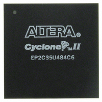
EP2C35U484C6 Altera, EP2C35U484C6 Datasheet - Page 145

EP2C35U484C6
Manufacturer Part Number
EP2C35U484C6
Description
IC CYCLONE II FPGA 33K 484-UBGA
Manufacturer
Altera
Series
Cyclone® IIr
Datasheet
1.EP2C5T144C8N.pdf
(168 pages)
Specifications of EP2C35U484C6
Number Of Logic Elements/cells
33216
Number Of Labs/clbs
2076
Total Ram Bits
483840
Number Of I /o
322
Voltage - Supply
1.15 V ~ 1.25 V
Mounting Type
Surface Mount
Operating Temperature
0°C ~ 85°C
Package / Case
484-UBGA
For Use With
P0301 - DE2 CALL FOR ACADEMIC PRICING544-1733 - PCI KIT W/CYCLONE II EP2C35N
Lead Free Status / RoHS Status
Contains lead / RoHS non-compliant
Number Of Gates
-
Other names
544-2112
Available stocks
Company
Part Number
Manufacturer
Quantity
Price
Company:
Part Number:
EP2C35U484C6
Manufacturer:
ALTERA10
Quantity:
65
Part Number:
EP2C35U484C6
Manufacturer:
ALTERA/阿尔特拉
Quantity:
20 000
Company:
Part Number:
EP2C35U484C6N
Manufacturer:
ALTERA
Quantity:
171
Altera Corporation
February 2008
SSTL_2_CLASS_I
SSTL_18_CLASS_I
High-speed clock
Duty cycle
High-speed I/O data rate
Time unit interval
Channel-to-channel skew
Table 5–46. Maximum Output Clock Toggle Rate Derating Factors (Part 4 of 4)
Table 5–47. High-Speed I/O Timing Definitions (Part 1 of 2)
I/O Standard
Parameter
OCT_50
_OHMS
OCT_50
_OHMS
Strength
f
t
HSIODR High-speed receiver and transmitter input and output data rate.
TUI
TCCS
H S C K L K
D U T Y
Symbol
Drive
High Speed I/O Timing Specifications
The timing analysis for LVDS, mini-LVDS, and RSDS is different
compared to other I/O standards because the data communication is
source-synchronous.
You should also consider board skew, cable skew, and clock jitter in your
calculation. This section provides details on the timing parameters for
high-speed I/O standards in Cyclone II devices.
Table 5–47
Figure
5–3.
Speed
Grade
High-speed receiver and transmitter input and output clock frequency.
Duty cycle on high-speed transmitter output clock.
TUI = 1/HSIODR.
The timing difference between the fastest and slowest output edges,
including t
TCCS measurement.
TCCS = TUI – SW – (2 × RSKM)
–6
67
30
Column I/O Pins
defines the parameters of the timing diagram shown in
Maximum Output Clock Toggle Rate Derating Factors (ps/pF)
Speed
Grade
–7
69
33
CO
variation and clock skew. The clock is included in the
Speed
Grade
–8
70
36
DC Characteristics and Timing Specifications
Speed
Grade
–6
25
47
Row I/O Pins
Description
Cyclone II Device Handbook, Volume 1
Speed
Grade
–7
42
49
Speed
Grade
–8
60
51
Speed
Grade
–6
25
47
Dedicated Clock
Outputs
Speed
Grade
–7
42
49
Speed
Grade
5–55
–8
60
51


