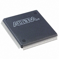
EPF81500AQC240-2 Altera, EPF81500AQC240-2 Datasheet - Page 7

EPF81500AQC240-2
Manufacturer Part Number
EPF81500AQC240-2
Description
IC FLEX 8000A FPGA 16K 240-PQFP
Manufacturer
Altera
Series
FLEX 8000r
Datasheet
1.EPF8282ATC100-3.pdf
(62 pages)
Specifications of EPF81500AQC240-2
Number Of Logic Elements/cells
1296
Number Of Labs/clbs
162
Number Of I /o
181
Number Of Gates
16000
Voltage - Supply
4.75 V ~ 5.25 V
Mounting Type
Surface Mount
Operating Temperature
0°C ~ 85°C
Package / Case
240-MQFP, 240-PQFP
Family Name
FLEX 8000
Number Of Usable Gates
16000
Number Of Logic Blocks/elements
1296
# Registers
1500
# I/os (max)
181
Frequency (max)
125MHz
Process Technology
CMOS
Operating Supply Voltage (typ)
5V
Logic Cells
1296
Ram Bits
8
Device System Gates
16000
Operating Supply Voltage (min)
4.75V
Operating Supply Voltage (max)
5.25V
Operating Temp Range
0C to 70C
Operating Temperature Classification
Commercial
Mounting
Surface Mount
Pin Count
240
Package Type
PQFP
Lead Free Status / RoHS Status
Contains lead / RoHS non-compliant
Total Ram Bits
-
Lead Free Status / Rohs Status
Not Compliant
Other names
544-2249
Available stocks
Company
Part Number
Manufacturer
Quantity
Price
Company:
Part Number:
EPF81500AQC240-2
Manufacturer:
ALTERA
Quantity:
135
Part Number:
EPF81500AQC240-2
Manufacturer:
ALTERA/阿尔特拉
Quantity:
20 000
Altera Corporation
Figure 3. FLEX 8000 LE
LABCTRL1
LABCTRL2
LABCTRL3
LABCTRL4
DATA1
DATA2
DATA3
DATA4
Each LAB provides four control signals that can be used in all eight LEs.
Two of these signals can be used as clocks, and the other two for
clear/preset control. The LAB control signals can be driven directly from
a dedicated input pin, an I/O pin, or any internal signal via the LAB local
interconnect. The dedicated inputs are typically used for global clock,
clear, or preset signals because they provide synchronous control with
very low skew across the device. FLEX 8000 devices support up to four
individual global clock, clear, or preset control signals. If logic is required
on a control signal, it can be generated in one or more LEs in any LAB and
driven into the local interconnect of the target LAB.
Logic Element
The logic element (LE) is the smallest unit of logic in the FLEX 8000
architecture, with a compact size that provides efficient logic utilization.
Each LE contains a 4-input LUT, a programmable flipflop, a carry chain,
and cascade chain.
The LUT is a function generator that can quickly compute any function of
four variables. The programmable flipflop in the LE can be configured for
D, T, JK, or SR operation. The clock, clear, and preset control signals on the
flipflop can be driven by dedicated input pins, general-purpose I/O pins,
or any internal logic. For purely combinatorial functions, the flipflop is
bypassed and the output of the LUT goes directly to the output of the LE.
Look-Up
Preset
Select
Clear/
Clock
(LUT)
Logic
Table
Carry-Out
Carry-In
Chain
Carry
FLEX 8000 Programmable Logic Device Family Data Sheet
Cascade-Out
Figure 3
Cascade-In
Cascade
Chain
shows a block diagram of an LE.
DFF
D
CLRN
PRN
Q
LE-Out
7
3


