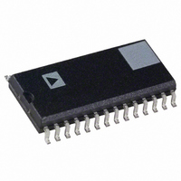
ADMCF326BR Analog Devices Inc, ADMCF326BR Datasheet - Page 6

ADMCF326BR
Manufacturer Part Number
ADMCF326BR
Description
IC DSP FLASH MOTOR CTRLR 28SOIC
Manufacturer
Analog Devices Inc
Series
Motor Controlr
Type
Fixed Pointr
Datasheet
1.ADMCF326BN.pdf
(36 pages)
Specifications of ADMCF326BR
Rohs Status
RoHS non-compliant
Interface
Synchronous Serial Port (SSP)
Clock Rate
20MHz
Non-volatile Memory
FLASH (12 kB), ROM (12kB)
On-chip Ram
2.5kB
Voltage - I/o
5.00V
Voltage - Core
5.00V
Operating Temperature
-40°C ~ 85°C
Mounting Type
Surface Mount
Package / Case
28-SOIC (7.5mm Width)
Available stocks
Company
Part Number
Manufacturer
Quantity
Price
Part Number:
ADMCF326BR
Manufacturer:
ADI/亚德诺
Quantity:
20 000
Company:
Part Number:
ADMCF326BRZ
Manufacturer:
SHARP
Quantity:
1 000
Part Number:
ADMCF326BRZ
Manufacturer:
ADI/亚德诺
Quantity:
20 000
ADMCF326
ABSOLUTE MAXIMUM RATINGS*
Supply Voltage (V
Input Voltage . . . . . . . . . . . . . . . . . . . . . –0.3 V to V
Output Voltage Swing . . . . . . . . . . . . . . –0.3 V to V
Flash Memory Erase or Program
Operating Temperature Range (Ambient) . . . –40°C to +85°C
Storage Temperature Range . . . . . . . . . . . . –65°C to +150°C
Lead Temperature (5 sec) . . . . . . . . . . . . . . . . . . . . . . . 280°C
Storage Temperature Range for SOIC Package . . –65°C to +150°C
Storage Temperature Range for PDIP Package . . –40°C to +125°C
*Stresses greater than those listed under Absolute Maximum Ratings may cause
Model
ADMCF326BR
ADMCF326BN
ADMCF326-EVALKIT
CAUTION
ESD (electrostatic discharge) sensitive device. Electrostatic charges as high as 4000 V readily
accumulate on the human body and test equipment and can discharge without detection. Although
the ADMCF326 features proprietary ESD protection circuitry, permanent damage may occur on
devices subjected to high energy electrostatic discharges. Therefore, proper ESD precautions are
recommended to avoid performance degradation or loss of functionality.
permanent damage to the device. These are stress ratings only; functional
operation of the device at these or any other conditions greater than those indicated
in the operational sections of this specification is not implied. Exposure to absolute
maximum rating conditions for extended periods may affect device reliability.
Temperature Range (Ambient) . . . . . . . . . . . . 0°C to 85°C
PIO6/CLKOUT
PIO3/SCLK1
PIO4/DR1A
PIO2/DR1B
PIO5/RFS1
PIO0/TFS1
PWMTRIP
PIO1/DT1
DD
PIN CONFIGURATION
CLKIN
XTAL
) . . . . . . . . . . . . . . . . . . –0.3 V to +7.0 V
V
DD
V3
V2
V1
10
11
12
13
14
1
2
3
4
5
6
7
8
9
(Not to Scale)
ADMCF326
TOP VIEW
Temperature
Range
–40°C to +85°C
–40°C to +85°C
28
27
26
25
24
23
22
21
20
19
18
17
16
15
PIO7/AUX1
PIO8/AUX0
AL
AH
BL
BH
CL
CH
RESET
GND
ICONST
VAUX2
VAUX1
VAUX0
DD
DD
ORDERING GUIDE
+ 0.3 V
+ 0.3 V
Instruction
Rate
20 MHz
20 MHz
–6–
Pin
No.
10
11
12
13
14
15
16
17
18
19
20
21
22
23
24
25
26
27
28
1
2
3
4
5
6
7
8
9
PIN FUNCTION DESCRIPTIONS
Package
Description
28-Lead Wide Body (SOIC)
28-Lead PDIP
Development Tool Kit
Pin
Name
PIO6/CLKOUT
PIO5/RFS1
PIO4/DR1A
PIO3/SCLK1
PIO2/DR1B
PIO1/DT1
PIO0/TFS1
CLKIN
XTAL
V
PWMTRIP
V3
V2
V1
VAUX0
VAUX1
VAUX2
ICONST
GND
RESET
CH
CL
BH
BL
AH
AL
PIO8/AUX0
PIO7/AUX1
DD
WARNING!
ESD SENSITIVE DEVICE
Pin
Type
I/O
I/O
I/O
I/O
I/O
I/O
I/O
I
O
SUP
I
I
I
I
I
I
I
O
GND
I
O
O
O
O
O
O
I/O
I/O
Package
Option
SO-28
N-28
REV. B


