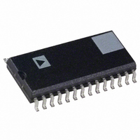
ADMCF326BR Analog Devices Inc, ADMCF326BR Datasheet - Page 21

ADMCF326BR
Manufacturer Part Number
ADMCF326BR
Description
IC DSP FLASH MOTOR CTRLR 28SOIC
Manufacturer
Analog Devices Inc
Series
Motor Controlr
Type
Fixed Pointr
Datasheet
1.ADMCF326BN.pdf
(36 pages)
Specifications of ADMCF326BR
Rohs Status
RoHS non-compliant
Interface
Synchronous Serial Port (SSP)
Clock Rate
20MHz
Non-volatile Memory
FLASH (12 kB), ROM (12kB)
On-chip Ram
2.5kB
Voltage - I/o
5.00V
Voltage - Core
5.00V
Operating Temperature
-40°C ~ 85°C
Mounting Type
Surface Mount
Package / Case
28-SOIC (7.5mm Width)
Available stocks
Company
Part Number
Manufacturer
Quantity
Price
Part Number:
ADMCF326BR
Manufacturer:
ADI/亚德诺
Quantity:
20 000
Company:
Part Number:
ADMCF326BRZ
Manufacturer:
SHARP
Quantity:
1 000
Part Number:
ADMCF326BRZ
Manufacturer:
ADI/亚德诺
Quantity:
20 000
Following power-on or reset, all bits of PIOINTEN0 and
PIOINTEN1 are cleared so that no interrupts are enabled.
Each PIO line has an internal pull-down resistor so that follow-
ing power-on or reset, all nine lines are configured as input PIOs
and will be read as logic lows if left unconnected.
Multiplexing of PIO Lines
The PIO0–PIO5 lines are multiplexed on the ADMCF326 with
the functional lines of the serial port, SPORT1. Although the
PIOSELECT Register permits individual selection of the func-
tionality of each pin, certain restrictions apply when using
SPORT1 for serial communications.
In general, when transmitting and receiving data on the DTI and
DRIB pins, respectively, the PIO0/TFS1 and PIO5/RFS1 pins
must also be selected for SPORT (TFS1 and RFS1) functional-
ity even if unframed communication is implemented. Therefore,
when using SPORT1 for any type of serial communication, the
minimal setting for PIOSELECT is 0xD8 (i.e., select DTI, DRIB,
RFS1 and TFS1, select PIO7, PIO6, PIO4, PIO3 as digital I/O).
If the serial port communications use an internally generated
SCLK1, the PIO3/SCLK1 pin may be used as a general-purpose
PIO line. When External SCLK Mode is selected, the PIO/SCLK1
pin must be enabled as SCLK1 (PIOSELECT [3] = 0).
When the DRIB data receive line of SPORT1 is selected as
the data receive line (MODECTRL [4] = 1), the PIO4/DRIA
line may be used as a general-purpose PIO pin. When the DRIA
data receive line of SPORT1 is selected as the data receive line
(MODECTRL [4] = 0), the PIO2/DRIB line may be used as
a general-purpose PIO pin.
The functionality of the PIO6/CLKOUT, PIO7/AUX1, and
PIO8/AUX0 pins may be selected on a pin-by-pin basis as desired.
PIO Registers
The configuration of all registers of the PIO system is shown at
the end of the data sheet.
INTERRUPT CONTROL
The ADMCF326 can respond to 16 different interrupt sources,
some of which are generated by internal DSP core interrupts
and others from the motor control peripherals. The DSP core
interrupts include the following:
·
·
·
·
The interrupts generated by the motor control peripherals include:
·
·
·
REV. B
AUXILIARY PWM TIMERS
Parameter
Resolution
PWM Frequency
A Peripheral (or IRQ2) Interrupt
A SPORT1 Receive (or IRQ0) and a SPORT1 Transmit (or
IRQ1) Interrupt
Two Software Interrupts
An Interval Timer Time-Out Interrupt
A PWMSYNC Interrupt
Nine Programmable Input/Output (PIO) Interrupts
A PWM Trip Interrupt
Table VIII. Auxiliary PWM Timer
Test Conditions
10 MHz CLKIN
–21–
The core interrupts are internally prioritized and individually
maskable. All peripheral interrupts are multiplexed into the DSP
core through the peripheral (IRQ2) interrupt.
The PWMSYNC interrupt is triggered by a low-to-high tran-
sition on the PWMSYNC pulse. The PWMTRIP interrupt is
triggered on a high-to-low transition on the PWMTRIP pin, or
by writing to the PWMSWT Register. A PIO interrupt is detected
on any change of state (high-to-low or low-to-high) on the
PIO lines.
The ADMCF326 interrupt control system is configured and
controlled by the IFC, IMASK, and ICNTL Registers of the
DSP core and by the IRQFLAG register for the PWMSYNC
and PWMTRIP interrupts. PIO interrupts are enabled and
disabled by the PIOINTEN0 and PIOINTEN1 Registers.
Interrupt Source
PWMTRIP
Peripheral Interrupt (IRQ2)
PWMSYNC
PIO
Software Interrupt 1
Software Interrupt 0
SPORT1 Transmit Interrupt (or IRQ1) 0x0020
SPORT1 Receive Interrupt (or IRQ0) 0x0024
Timer
Interrupt Masking
Interrupt masking (or disabling) is controlled by the IMASK
register of the DSP core. This register contains individual bits
that must be set to enable the various interrupt sources. If any
peripheral interrupt (PWMSYNC, PWMTRIP, or PIO) is to
be enabled, the IRQ2 interrupt enable bit (Bit 9) of the IMASK
Register must be set. The configuration of the IMASK Register
of the ADMCF326 is shown at the end of the data sheet.
Interrupt Configuration
The IFC and ICNTL Registers of the DSP core control and con-
figure the interrupt controller of the DSP core. The IFC register is
a 16-bit register that may be used to force and/or clear any of
the eight DSP interrupts. Bits 0 to 7 of the IFC register may
be used to clear the DSP interrupts while Bits 8 to 15 can be
used to force a corresponding interrupt. Writing to Bits 11 and 12
in IFC is the only way to create the two software interrupts.
The ICNTL register is used to configure the sensitivity (edge
or level) of the IRQ0, IRQ1, and IRQ2 interrupts and to enable/
disable interrupt nesting. Setting Bit 0 of ICNTL configures the
IRQ0 as edge-sensitive, while clearing the bit configures it for
level-sensitive. Bit 1 is used to configure the IRQ1 interrupt.
Table IX. Interrupt Vector Addresses
Min
0.039
Typ
8
Interrupt Vector Address
0x002C (Highest Priority)
0x0004
0x000C
0x0008
0x0018
0x001C
0x0028 (Lowest Priority)
Max
ADMCF326
Unit
Bits
MHz


