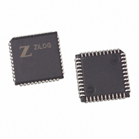
Z8927320VSG Zilog, Z8927320VSG Datasheet - Page 39

Z8927320VSG
Manufacturer Part Number
Z8927320VSG
Description
DSP 20MHZ 16-BIT W/ A/D 44-PLCC
Manufacturer
Zilog
Series
Z892x3r
Type
Fixed Pointr
Datasheet
1.Z8937320FSC00TR.pdf
(60 pages)
Specifications of Z8927320VSG
Interface
SPI, 3-Wire Serial
Clock Rate
20MHz
Non-volatile Memory
OTP (16 kB)
On-chip Ram
1kB
Voltage - I/o
5.00V
Voltage - Core
5.00V
Operating Temperature
0°C ~ 70°C
Mounting Type
Surface Mount
Package / Case
44-LCC (J-Lead)
Lead Free Status / RoHS Status
Lead free / RoHS Compliant
Available stocks
Company
Part Number
Manufacturer
Quantity
Price
Company:
Part Number:
Z8927320VSG
Manufacturer:
Zilog
Quantity:
50
ZiLOG
DS000202-DSP0599
Bank13/EXT0 (LSB)
D7 D6 D5 D4 D3 D2 D1 D0
QUAD
DIV2
0
0
1
1
0
0
0
0
1
1
1
1
Table 18. A/D Prescaler Values (Bits 7, 6, 5)
CSEL1
Table 19. Operating Modes (Bits 4, 3)
0
0
1
1
Table 20. Channel Select (Bits 1, 0)
Figure 29. ADCTL Register (LSB)
SCAN
DIV1
0
1
0
1
0
0
1
1
0
0
1
1
Option
Convert selected channel 4 times,
then stop
Convert selected channel,
then stop.
Convert 4 channels,
then stop.
Convert 4 channels
continuously.
DIV0
CSEL0
0
1
0
1
0
1
0
1
0
1
0
1
(Reserved)
CSEL0
CSEL1
SCAN
QUAD
DIV0
DIV1
DIV2
(Crystal divided by)
A/D Prescaler
Channel
16
24
32
40
48
56
64
8
AN0
AN1
AN2
AN3
ADE (Bit 15).
cessing any A/D registers, except writing to the ADE bit.
A “1” enables all A/D accesses.
Reserved (Bits 14, 13).
ADCINT (Bit 12).
ADCINT will reset every time this register is written.
ADIT (Bit 11).
terrupts are enabled (ADIE=1). A value of “0” sets the in-
terrupt after the first A/D conversion is complete. A value
of “1” sets the interrupt after the fourth A/D conversion is
complete.
ADIE (Bit 10).
ables the A/D Interrupt. A value of “1” enables the A/D In-
terrupt.
There are four A/D result registers. See the EXT Register
Assignments for their location in the different banks.
Bank13/EXT0 (MSB)
ADST1
D15 D14 D13 D12 D11 D10 D9 D8
16-Bit Digital Signal Processors with A/D Converter
0
0
1
1
Figure 30. ADCTL Register (MSB)
A “0” disables any A/D conversions or ac-
ADST0
Table 21. START (Bits 9, 8)
Selects when to set the A/D interrupt if in-
A/D Interrupt Enable. A value of “0” dis-
0
1
0
1
The A/D interrupt bit is read-only. The
Reserved for future use.
Option
Conversion starts when this
register is written.
Conversion starts on INT1 per
Interrupt Allocation Register
Conversion starts on C/T2
time-out.
Conversion starts on C/T0
time-out.
Z89223/273/323/373
ADST0
ADST1
ADIE
ADIT
ADCINT
(Reserved)
ADE
39


