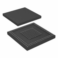
ADSP-BF527KBCZ-6C2 Analog Devices Inc, ADSP-BF527KBCZ-6C2 Datasheet - Page 6

ADSP-BF527KBCZ-6C2
Manufacturer Part Number
ADSP-BF527KBCZ-6C2
Description
IC DSP 16BIT 600MHZ 289CSPBGA
Manufacturer
Analog Devices Inc
Series
Blackfin®r
Type
Fixed Pointr
Datasheets
1.ADSP-BF531SBSTZ400.pdf
(12 pages)
2.ADSP-BF523BBCZ-5A.pdf
(88 pages)
3.ADSP-BF523KBCZ-5C2.pdf
(36 pages)
Specifications of ADSP-BF527KBCZ-6C2
Package / Case
289-CSPBGA
Interface
DMA, Ethernet, I²C, PPI, SPI, SPORT, UART, USB
Clock Rate
600MHz
Non-volatile Memory
ROM (32 kB)
On-chip Ram
132kB
Voltage - I/o
1.8V, 2.5V, 3.3V
Voltage - Core
1.10V
Operating Temperature
0°C ~ 70°C
Mounting Type
Surface Mount
Svhc
No SVHC (18-Jun-2010)
Cache On Chip L1/l2 Memory
48KB
Core Frequency Typ
600MHz
Dsp Type
Core
External Supported Memory
SDRAM, SRAM, FLASH, ROM
Interface Type
SPI, Parallel, 2 Wire
Rohs Compliant
Yes
Mmac
1200
No. Of Pins
289
Package
289CSP-BGA
Maximum Speed
600 MHz
Lead Free Status / RoHS Status
Lead free / RoHS Compliant
For Use With
ADZS-BF527-MPSKIT - BOARD EVAL MEDIA PLAYER BF527ADZS-BF527-EZLITE - BOARD EVAL ADSP-BF527
Lead Free Status / RoHS Status
Lead free / RoHS Compliant, Lead free / RoHS Compliant
Available stocks
Company
Part Number
Manufacturer
Quantity
Price
Company:
Part Number:
ADSP-BF527KBCZ-6C2
Manufacturer:
Analog Devices Inc
Quantity:
10 000
The programmer can simultaneously load the volume control of
both channels by writing to the LRHPBOTH (Register R2, Bit
D8) and RLHPBOTH (Register R3, Bit D8) bits of the left- or
right-channel DAC volume registers.
The maximum output level of the headphone outputs is
1.0 V rms when AVDD and HPVDD = 3.3 V. To suppress audi-
ble pops and clicks, the headphone and line outputs are held at
the VMID dc voltage level when the device is set to standby
mode or when the headphone outputs are muted.
The stereo line outputs of the codec, the LOUT and ROUT pins,
can drive a load impedance of 10 kΩ and 50 pF. The line output
signal levels are not adjustable at the output mixer, which has a
fixed gain of 0 dB. The maximum output level of the line out-
puts is 1.0 V rms when AVDD = 3.3 V.
CODEC_BCLK
CODEC_BCLK
ADSP-BF522C/ADSP-BF523C/ADSP-BF524C/ADSP-BF525C/ADSP-BF526C/ADSP-BF527C
X = DON’T CARE.
ADCLRC/
ADCDAT/
X = DON’T CARE.
ADCLRC/
ADCDAT/
DACLRC
DACDAT
DACLRC
DACDAT
1
X
2
X
3
N
4
LEFT CHANNEL
LEFT CHANNEL
Figure 7. Right-Justified Audio Input Mode
Figure 6. Left-Justified Audio Input Mode
Rev. A | Page 6 of 36 | March 2010
4
N
3
X
2
1/
1/
f
f
S
S
X
1
DIGITAL AUDIO INTERFACE
The digital audio input can support the following digital audio
communication protocols: right-justified mode, left-justified
mode, I
through
The mode selection is performed by writing to the FORMAT
bits of the digital audio interface register (Register R7, Bit D1
and Bit D0). All modes are MSB first and operate with data of 16
to 32 bits.
1
X
2
X
2
S mode, and frame sync mode. See
Figure 10 on Page
3
N
RIGHT CHANNEL
RIGHT CHANNEL
4
7.
N
3
X
2
X
1
Figure 6 on Page 6


