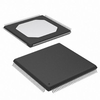
XC95288XL-10TQG144C Xilinx Inc, XC95288XL-10TQG144C Datasheet - Page 16

XC95288XL-10TQG144C
Manufacturer Part Number
XC95288XL-10TQG144C
Description
IC CPLD 6.4K 288MCELL 144-TQFP
Manufacturer
Xilinx Inc
Series
XC9500XLr
Specifications of XC95288XL-10TQG144C
Programmable Type
In System Programmable (min 10K program/erase cycles)
Delay Time Tpd(1) Max
10.0ns
Voltage Supply - Internal
3 V ~ 3.6 V
Number Of Logic Elements/blocks
16
Number Of Macrocells
288
Number Of Gates
6400
Number Of I /o
117
Operating Temperature
0°C ~ 70°C
Mounting Type
Surface Mount
Package / Case
144-TQFP, 144-VQFP
Voltage
3.3V
Memory Type
FLASH
Lead Free Status / RoHS Status
Lead free / RoHS Compliant
Features
-
Number Of Logic Elements/cells
-
Other names
122-1381
Available stocks
Company
Part Number
Manufacturer
Quantity
Price
Company:
Part Number:
XC95288XL-10TQG144C
Manufacturer:
XILINX
Quantity:
513
Company:
Part Number:
XC95288XL-10TQG144C
Manufacturer:
Xilinx Inc
Quantity:
10 000
Part Number:
XC95288XL-10TQG144C
Manufacturer:
XILINX/赛灵思
Quantity:
20 000
Company:
Part Number:
XC95288XL-10TQG144C.
Manufacturer:
XILINX
Quantity:
1 831
Power-Up Characteristics
During power-up, the XC9500XL device I/Os may be unde-
fined until V
called the subthreshold
fully turned on. If V
with V
range. If V
the subthreshold region, I/Os will be in 3-state with a weak
pull-up until V
ation state (approximately 2.5V). When V
point, user registers are initialized (typically within 200 μs)
after which I/Os will assume the behavior determined by the
user pattern, as shown in
If the device is in the erased state (before any user pattern
is programmed), the device outputs remain disabled with
weak pull-up. The JTAG pins are enabled to allow the device
to be programmed at any time. All devices are shipped in
the erased state from the factory.
If the device is programmed, the device inputs and outputs
take on their configured states for normal operation. The
JTAG pins are enabled to allow device erasure or bound-
ary-scan tests at any time.
Development System Support
The XC9500XL family and associated in-system program-
ming capabilities are fully supported in either software solu-
tions available from Xilinx.
The Foundation Series is an all-in-one development system
containing schematic entry, HDL (VHDL, Verilog, and
Table 4: Timing Model Parameters
Table 5: XC9500XL Pin Characteristics
DS054 (v2.5) May 22, 2009
Product Specification
Notes:
1.
IOB Bus-Hold
Device I/O and Clocks
JTAG Controller
Parameter
T
SYSTEM
S = the logic span of the function, as defined in the text.
T
T
T
T
T
Device Circuitry
PSU
PCO
CCINT
CO
PD
SU
CCIO
, I/Os may drive during this voltage transition
R
CCINT
CCINT
is powered after V
Propagation Delay
Global Clock Setup Time
Global Clock-to-output
Product Term Clock Setup Time
Product Term Clock-to-output
Internal System Cycle Period
CCIO
rises above 1 Volt. This time period is
reaches the threshold of the User Oper-
is powered before or simultaneously
region,
Figure
Description
Subthreshold State
as transistors have not yet
17.
CCINT
Undetermined
Undetermined
Undetermined
has passed through
CCINT
reaches this
www.xilinx.com
Quiescent State
Product Term
Allocator
+ T
+ T
+ T
+ T
Disabled
Disabled
Pull-up
PTA
PTA
PTA
PTA
-
-
ABEL), and simulation capabilities. It supports the
XC9500XL family as well as other CPLD and FPGA fami-
lies.
The Alliance Series includes CPLD and FPGA implementa-
tion technology as well as all necessary libraries and inter-
faces for Alliance partner EDA solutions.
FastFLASH Technology
An advanced 0.35 micron feature size CMOS Flash process is
used to fabricate all XC9500XL devices. The FastFLASH pro-
cess provides high performance logic capability, fast pro-
gramming times, and superior reliability and endurance
ratings.
XC9500XL High-Performance CPLD Family Data Sheet
Subthreshold
*
*
*
*
S
S
S
S
(1)
State
3.8 V
(Typ)
1.0V
2.5V
(Typ)
Figure 17: Device Behavior During Power-up
0V
V
Power
CCINT
No
Low-Power Setting
Erased Device
Quiescent
Macrocell
Operation
State
Disabled
Enabled
Pull-up
+ T
+ T
+ T
+ T
-
-
LP
LP
LP
LP
Initialization of User Registers
User Operation
Output Slew-Limited
Valid User Operation
As Configured
Bus-Hold
+ T
+ T
+ T
Setting
Enabled
Quiescent
State
SLEW
SLEW
SLEW
–
-
-
DS054_17_042101
Power
No
16


