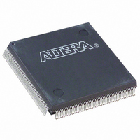
EPM3256AQC208-10N Altera, EPM3256AQC208-10N Datasheet - Page 7

EPM3256AQC208-10N
Manufacturer Part Number
EPM3256AQC208-10N
Description
IC MAX 3000A CPLD 256 208-PQFP
Manufacturer
Altera
Series
MAX® 3000Ar
Datasheet
1.EPM3032ATC44-10N.pdf
(46 pages)
Specifications of EPM3256AQC208-10N
Programmable Type
In System Programmable
Delay Time Tpd(1) Max
10.0ns
Voltage Supply - Internal
3 V ~ 3.6 V
Number Of Logic Elements/blocks
16
Number Of Macrocells
256
Number Of Gates
5000
Number Of I /o
158
Operating Temperature
0°C ~ 85°C
Mounting Type
Surface Mount
Package / Case
208-MQFP, 208-PQFP
Voltage
3.0 V ~ 3.6 V
Memory Type
EEPROM
Number Of Logic Elements/cells
16
Family Name
MAX 3000A
# Macrocells
256
Number Of Usable Gates
5000
Frequency (max)
125MHz
Propagation Delay Time
10ns
Number Of Logic Blocks/elements
16
# I/os (max)
158
Operating Supply Voltage (typ)
3.3V
In System Programmable
Yes
Operating Supply Voltage (min)
3V
Operating Supply Voltage (max)
3.6V
Operating Temp Range
0C to 70C
Operating Temperature Classification
Commercial
Mounting
Surface Mount
Pin Count
208
Package Type
PQFP
Lead Free Status / RoHS Status
Lead free / RoHS Compliant
Features
-
Lead Free Status / Rohs Status
Compliant
Other names
544-1988
EPM3256AQC208-10N
EPM3256AQC208-10N
Available stocks
Company
Part Number
Manufacturer
Quantity
Price
Company:
Part Number:
EPM3256AQC208-10N
Manufacturer:
ALTERA52
Quantity:
4 054
Altera Corporation
For registered functions, each macrocell flipflop can be individually
programmed to implement D, T, JK, or SR operation with programmable
clock control. The flipflop can be bypassed for combinatorial operation.
During design entry, the designer specifies the desired flipflop type; the
Altera development system software then selects the most efficient
flipflop operation for each registered function to optimize resource
utilization.
Each programmable register can be clocked in three different modes:
■
■
■
Two global clock signals are available in MAX 3000A devices. As shown
in
either of the two global clock pins, GCLK1 or GCLK2.
Each register also supports asynchronous preset and clear functions. As
shown in
to control these operations. Although the product–term–driven preset
and clear from the register are active high, active–low control can be
obtained by inverting the signal within the logic array. In addition, each
register clear function can be individually driven by the active–low
dedicated global clear pin (GCLRn).
All registers are cleared upon power-up. By default, all registered outputs
drive low when the device is powered up. You can set the registered
outputs to drive high upon power-up through the Quartus
Quartus II software uses the NOT Gate Push-Back method, which uses an
additional macrocell to set the output high. To set this in the Quartus II
software, go to the Assignment Editor and set the Power-Up Level
assignment for the register to High.
Figure
Global clock signal mode, which achieves the fastest clock–to–output
performance.
Global clock signal enabled by an active–high clock enable. A clock
enable is generated by a product term. This mode provides an enable
on each flipflop while still achieving the fast clock–to–output
performance of the global clock.
Array clock implemented with a product term. In this mode, the
flipflop can be clocked by signals from buried macrocells or I/O pins.
1, these global clock signals can be the true or the complement of
Figure
2, the product–term select matrix allocates product terms
MAX 3000A Programmable Logic Device Family Data Sheet
®
II software.
7


