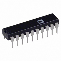
AD7112CN Analog Devices Inc, AD7112CN Datasheet - Page 7

AD7112CN
Manufacturer Part Number
AD7112CN
Description
IC DAC DUAL LOGARITHMIC 20-DIP
Manufacturer
Analog Devices Inc
Series
LOGDAC®r
Datasheet
1.AD7112BN.pdf
(12 pages)
Specifications of AD7112CN
Rohs Status
RoHS non-compliant
Number Of Bits
17
Data Interface
Parallel
Number Of Converters
2
Voltage Supply Source
Single Supply
Power Dissipation (max)
10mW
Operating Temperature
-40°C ~ 85°C
Mounting Type
Through Hole
Package / Case
20-DIP (0.300", 7.62mm)
Settling Time
-
TYPICAL PERFORMANCE CHARACTERISTICS
REV. 0
Another error arises from the output amplifier’s input offset volt-
age. The amplifier is operated with a fixed feedback resistance,
but the equivalent source impedance (the AD7112 output im-
pedance) varies as a function of the attenuation level. This has
the effect of varying the noise gain of the amplifier thus creating
a varying error due to amplifier offset voltage. It is recom-
mended that an amplifier with less than 50 V of input offset be
used (such as the AD712 or ADOP07) in dc applications. Am-
plifiers with a large input offset voltage may cause audible
thumps in audio applications due to dc output changes. The
100
100
0%
90
10
90
10
0%
Figure 4. Response of AD7112 with AD712
Figure 5. Response of AD7112 with OP275
5V
A1
5V
A1
0.8V
0.8V
5V
5V
200ns
200ns
DATA CHANGE
FROM 00H TO 80H
C1 = 0pF
C1 = 0pF
DATA CHANGE
FROM 00H TO 80H
C1 = 15pF
C1 = 15pF
–7–
AD7112 accuracy is specified and tested using only the internal
feedback resistor. Any gain error (i.e., mismatch of R
R–2R ladder) that may exist in the AD7112 D/A converter cir-
cuit results in a constant attenuation error over the whole range.
The AD7112 accuracy is specified relative to 0 dB attenuation,
hence gain trim resistors can be used to adjust V
cisely (i.e., 0 dB attenuation) with input code 00000000. For
further information on gain error refer to the “CMOS DAC Ap-
plication Guide” which is available from Analog Devices, Publi-
cation Number G872b-8-1/89.
Figure 7. Frequency Response with AD712 and OP275
Figure 6. Supply Current vs. Logic Input Level
–10
–20
–30
10
6
5
4
3
2
1
0
0
10
0
4
V
T
DATA INPUT CODE = 0000 0000
V
DD
A
IN
= +25
= 1V rms
= +5V
°
1
C
OP275
C1 = 15pF
10
5
FREQUENCY – Hz
2
V
OP275
C1 = 0pF
IN
T
ALL DIGITAL INPUTS
TIED TOGETHER
– Volts
A
AD712
C1 = 0pF
= +25
3
°
C
AD712
C1 = 15pF
10
6
AD7112
4
OUT
= V
FB
to the
IN
10
5
7
pre-


