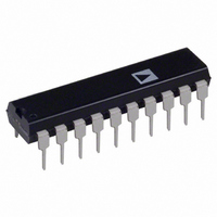
AD7112CN Analog Devices Inc, AD7112CN Datasheet - Page 11

AD7112CN
Manufacturer Part Number
AD7112CN
Description
IC DAC DUAL LOGARITHMIC 20-DIP
Manufacturer
Analog Devices Inc
Series
LOGDAC®r
Datasheet
1.AD7112BN.pdf
(12 pages)
Specifications of AD7112CN
Rohs Status
RoHS non-compliant
Number Of Bits
17
Data Interface
Parallel
Number Of Converters
2
Voltage Supply Source
Single Supply
Power Dissipation (max)
10mW
Operating Temperature
-40°C ~ 85°C
Mounting Type
Through Hole
Package / Case
20-DIP (0.300", 7.62mm)
Settling Time
-
REV. 0
Programmable State Variable Filter
The AD7112 with its multiplying capability and fast settling
time is ideal for many types of signal conditioning applications.
The circuit of Figure 22 shows its use in a state variable filter
design. This type of filter has three outputs: low pass, bandpass
and high pass. The particular version shown in Figure 22 uses
two AD7112 to control the critical parameters f
stead of several fixed resistors, the circuit uses the DAC equiva-
lent resistances as circuit elements. Thus, R1 in Figure 22 is
controlled by the 8-bit word loaded to DAC A1 of the AD7112.
This is also the case with R2, R3 and R4.
INPUT
Figure 21. Automatic Gain Control System
V
UP/DOWN COUNTER
IN
CONTROL LOGIC
GAIN ELEMENT
END STOP AND
U
1/2 AD7112
VARIABLE
V
IN
A
AD7112
D
DB0–DB7
DAC A1
DATA 1
(R1)
OUT A
NOTES
1. A1, A2, A3, A4 : 1/4 x AD713
2. C3 IS A COMPENSATION CAPACITOR TO ELIMINATE Q AND GAIN VARIATIONS
COMPARATOR
CAUSED BY AMPLIFIER GAIN BANDWIDTH LIMITATIONS
DETECTOR
OUT B
CS
A1
Figure 22. Programmable State Variable Filter
10k
R5
DAC B1
(R2)
R6
WR
R
0
, Q and A
FB
DAC A/
DAC B
B
30k
R8
A2
V
OUTPUT
V
REF
IN
B
0
V
. In-
IN
A
HIGH
PASS
OUTPUT
–11–
30k
AD7112
10pF
R7
DAC A2
DB0–DB7
C3
DATA 2
(R3)
DAC Equivalent Resistance,
where:
DACs A1 and B1 control the gain and Q of the filter character-
istic while DACs A2 and B2 control the cutoff frequency.
Circuit equations:
Programmable range for component values shown is f
to 15 kHz and Q = 0.3 to 4.5.
OUT A
R
N is the DAC code in Decimal (0 N 240).
C1 = C2, R3 = R4, R7 = R8.
Resonant frequency, f
Quality factor, Q = (R6/R8)
R
Bandpass Gain, A
DAC
FBB1
is the DAC ladder resistance.
is the feedback resistance of DAC B1 in Figure 22
V
1000pF
CS
IN
C1
A3
B
DAC B2
R
(R4)
WR
EQ
OUT B
DAC A/
DAC B
10
0
= –R2/R1.
0
= 1/(2
1000pF
EXP (–0.375
C2
A4
R
(R2/R
DAC
R3C1).
FBB1
LOW-PASS
OUTPUT
BANDPASS
OUTPUT
).
N / 20)
AD7112
0
= 0 kHz


