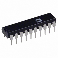
AD7112CN Analog Devices Inc, AD7112CN Datasheet - Page 6

AD7112CN
Manufacturer Part Number
AD7112CN
Description
IC DAC DUAL LOGARITHMIC 20-DIP
Manufacturer
Analog Devices Inc
Series
LOGDAC®r
Datasheet
1.AD7112BN.pdf
(12 pages)
Specifications of AD7112CN
Rohs Status
RoHS non-compliant
Number Of Bits
17
Data Interface
Parallel
Number Of Converters
2
Voltage Supply Source
Single Supply
Power Dissipation (max)
10mW
Operating Temperature
-40°C ~ 85°C
Mounting Type
Through Hole
Package / Case
20-DIP (0.300", 7.62mm)
Settling Time
-
AD7112
INTERFACE LOGIC INFORMATION
DAC Selection
Both DAC latches share a common 8-bit port. The control in-
put DAC A/DAC B selects which DAC can accept data from
the input port.
Mode Selection
Inputs CS and WR control the operating mode of the selected
DAC. See the Mode Selection Table below.
Write Mode
When CS and WR are both low the DAC is in the write mode.
The input data latches of the selected DAC are transparent and
its analog output responds to activity on DB0–DB7.
Hold Mode
The selected DAC latch retains the data which was present on
DB0–DB7 just prior to CS and WR assuming a high state. Both
analog outputs remain at the values corresponding to the data in
their respective latches.
DACA/
DAC B
L
H
X
X
L = Low State, V
DAC A/DAC B
DB0–DB7
NOTES
1. ALL INPUT SIGNAL RISE AND FALL TIMES MEASURED FROM
2. CONTROL TIMING MEASUREMENT REFERENCE LEVEL = (V
10% TO 90% OF V
WR
CS
Figure 3. Write Cycle Timing Diagram
IL
CS
L
L
H
X
; H = High State, V
t
Mode Selection Table
AS
DD
.
t
R
=
t
t
CS
WR
L
L
X
H
F = 20ns.
IH
; X = Don’t Care.
V
V
IH
IL
t
WR
DAC A
WRITE
HOLD
HOLD
HOLD
t
DS
t
AH
t
IH
DH
+ V
DAC B
HOLD
WRITE
HOLD
HOLD
t
CH
IL
) / 2
–6–
DYNAMIC PERFORMANCE
The dynamic performance of the AD7112 will depend on the
gain and phase characteristics of the output amplifier, together
with the optimum choice of PC board layout and decoupling
components. Circuit layout is most important if the optimum
performance of the AD7112 is to be achieved. Most application
problems stem from either poor layout, grounding errors, or in-
appropriate choice of amplifier. Ensure that the layout of the
printed circuit board has the digital and analog lines separated
as much as possible. Take care not to run any digital track
alongside an analog signal track. Establish a single point analog
ground (star ground) separate from the logic system ground.
Place this ground as close as possible to the AD7112. Connect
all analog grounds to this star ground, and also connect the
AD7112 DGND to this ground. Do not connect any other digi-
tal grounds to this analog ground point. Low impedance analog
and digital power supply common returns are essential for low
noise and high performance of these converters, therefore the
foil width of these tracks should be as wide as possible. The use
of ground planes is recommended as this minimizes impedance
paths and also guards the analog circuitry from digital noise.
It is recommended that when using the AD7112 with a high
speed amplifier, a capacitor (C1) be connected in the feedback
path as shown in Figure 2. This capacitor which should be be-
tween 5 pF and 15 pF, compensates for the phase lag intro-
duced by the output capacitance of the D/A converter. Figures
4 and 5 show the performance of the AD7112 using the
AD712, a high speed, low cost BiFET amplifier, and the
OP275, a dual bipolar/JFET amplifier suitable for audio appli-
cations. The performance with and without the compensation
capacitor is shown in both cases. For operation beyond
250 kHz, capacitor C1 may be reduced in value. This gives an
increase in bandwidth at the expense of a poorer transient re-
sponse as shown in Figure 7. In circuits where C1 is not in-
cluded, the high frequency roll-off point is primarily determined
by the characteristics of the output amplifier and not the AD7112.
Feedthrough and accuracy are sensitive to output leakage cur-
rents effects. For this reason it is recommended that the operat-
ing temperature of the AD7112 be kept as close to +25 C as is
practically possible, particularly where the devices performance
at high attenuation levels is important. A typical plot of leakage
current vs. temperature is shown in Figure 11.
Some solder fluxes and cleaning materials can form slightly
conductive films which cause leakage effects between analog in-
put and output. The user is cautioned to ensure that the manu-
facturing process for circuits using the AD7112 does not allow
such films to form. Otherwise the feedthrough, accuracy and
maximum usable range will be affected.
STATIC ACCURACY PERFORMANCE
The D/A converter section of the AD7112 consists of a 17-bit
this level of resolution it is necessary to pay great attention to
amplifier selection, circuit grounding, etc.
Amplifier input bias current results in a dc offset at the output
of the amplifier due to current flowing in the feedback resistor
R
of less than 10 nA be used (e.g., AD712) to minimize this offset.
R–2R type converter. To obtain optimum static performance at
FB
. It is recommended that amplifiers with input bias currents
REV. 0


